
 中文简体
中文简体 русский
 Español
 عربى
عربى Português
 日本語
日本語 한국어
한국어
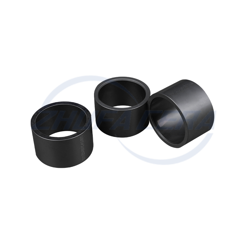
Black silicon carbide ceramic ring is a high-performance engineered ceramic assembly made of high-purity silicon carbide by precision molding and high temperature sintering. Its quadrangular crystal s...
See Details
FOLLOW US :


 Email: zf@zfcera.com
 Telephone: +86-188 8878 5188

"Hard-core base" for semiconductor equipment
2026-04-21
1. An all-rounder from cavity protection to precision load bearing2. Peak performance of thermal management and electrostatic adsorption3. Resilient support of the micro world4. The transition between domestic substitution and high purificationConclusion |
Related products
-
-
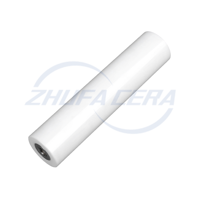
Zirconia Ceramic Rod is a high-performance ceramic material rod, mainly made of zirconium oxide, with excellent mechanical strength and chemical stability. It exhibits extremely high hardness and wear...
See Details -
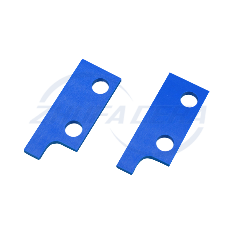
Blue zirconia ceramic sheets are precision components made of advanced zirconia ceramics. They are stained with cobalt, iron or copper to form a blue color. This color not only serves as a visual i...
See Details -

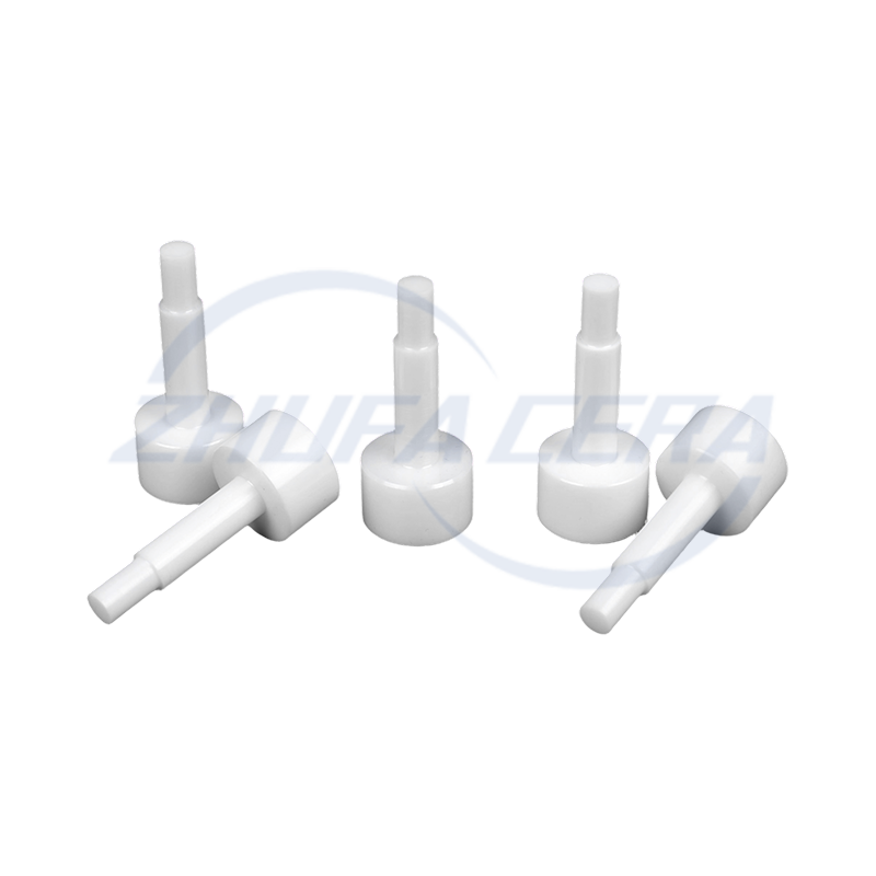
This blue zirconia ceramic pin is made of advanced zirconia ceramic material, providing excellent durability and performance. Zirconia ceramics are known for their high strength, good wear resistan...
See Details -

Zirconia Ceramic Gear is made of zirconium oxide ceramic material, which has excellent high strength and high hardness. This material property enables it to effectively resist wear during the transmis...
See Details -
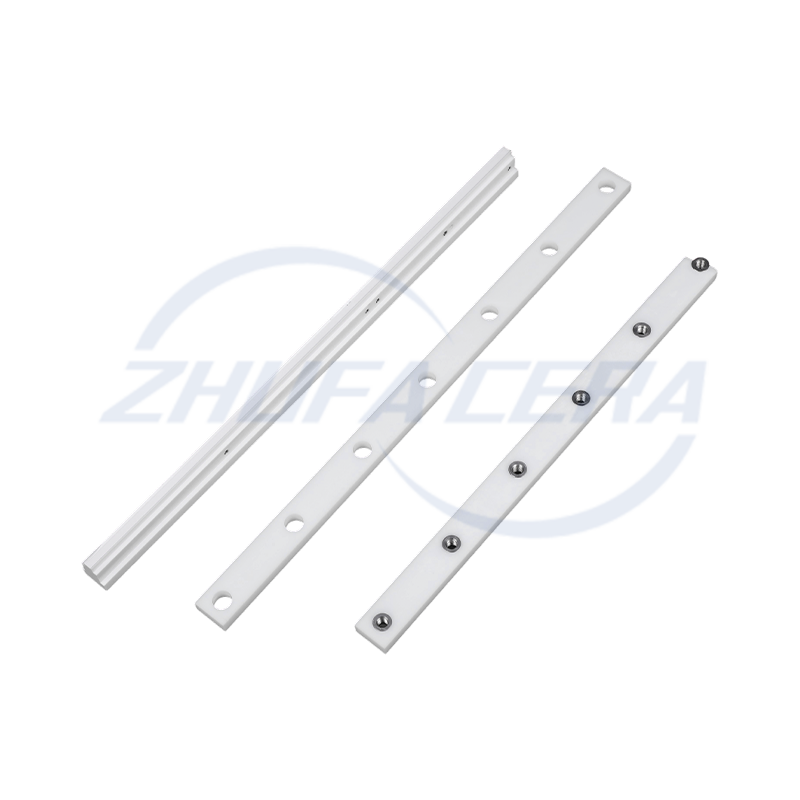
Zirconia Ceramic Guide Rail is a high-performance precision mechanical component made of zirconium oxide ceramic material. Its core characteristics are derived from the excellent physical and chemical...
See Details -
Zirconia Ceramic Locating Pin is a high-precision positioning element made of advanced zirconium oxide ceramic material with excellent physical and chemical properties. Its main characteristics includ...
See Details -
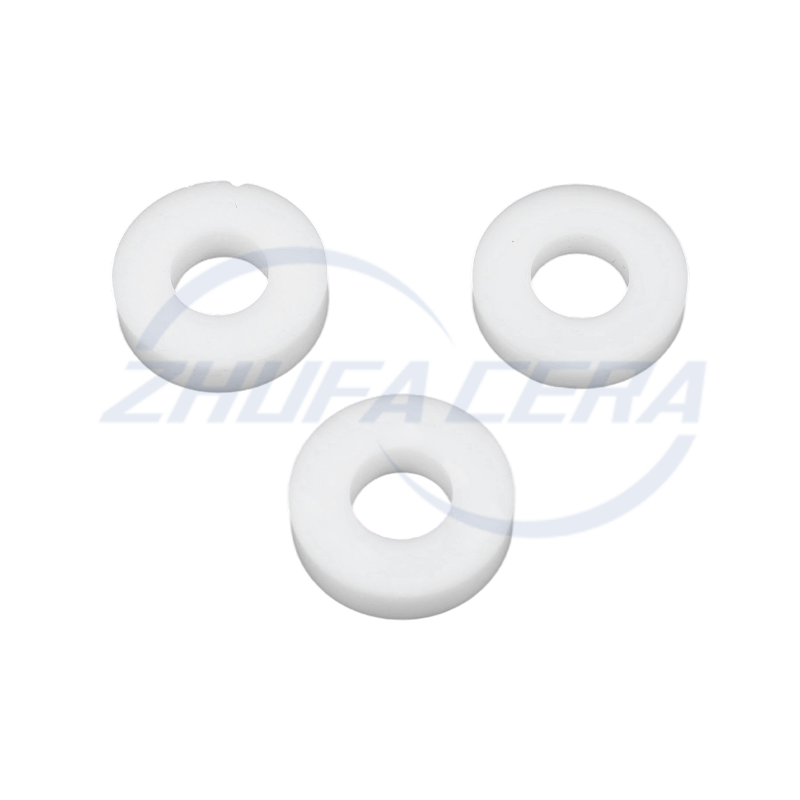
Zirconia Ceramic Ring is a high-performance ceramic product known for its excellent physical and chemical properties. It has extremely high hardness and strength, with a Mohs hardness of more than 8.5...
See Details -
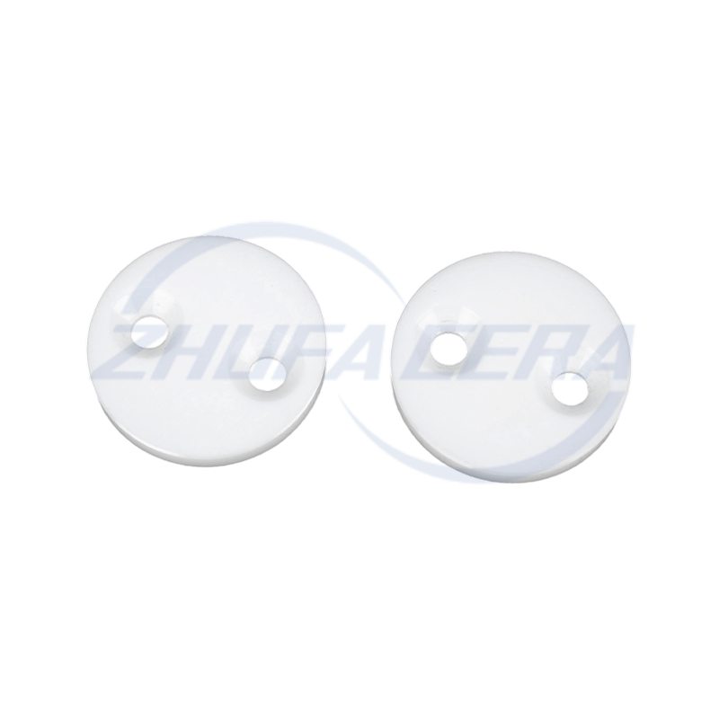
Zirconia ceramic sheets have become functional core components in various fields thanks to their unique properties. With a flexural strength of 900–1200 MPa and a fracture toughness of 6–10 MPa・m¹/², ...
See Details -

Zirconia Ceramic Strip is a strip material made of high-performance zirconium oxide ceramic with excellent physical and chemical properties. It has extremely high hardness and flexural strength, can e...
See Details -
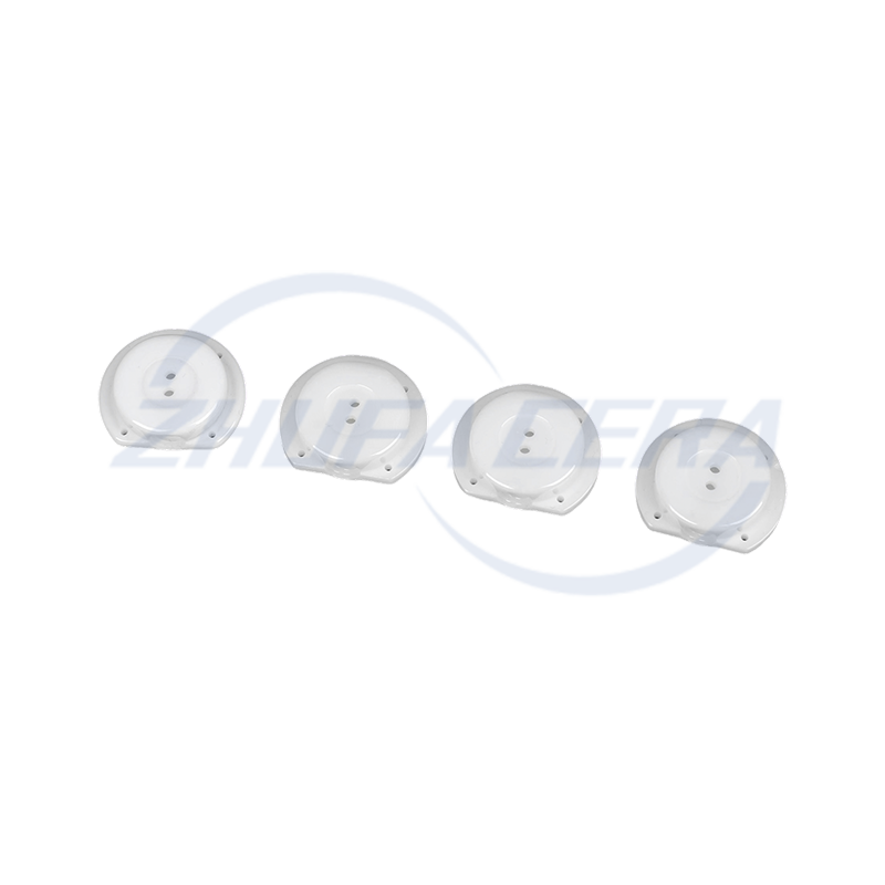
Zirconia ceramic wafers are representative products in the field of high-performance structural ceramics. Compared with traditional alumina ceramics or metal materials, its comprehensive performanc...
See Details -
Zirconia Ceramic Plunger is a high-performance component designed for harsh industrial environments. Compared with similar ceramic or metal plunger products, it stands out with its unique material adv...
See Details

-
Quick Links
Home Products About Us Services Technology News Contact Us -
Products
Ceramic Structural Parts Zirconia Ceramics Alumina Ceramics ZTA Ceramics Silicon Nitride Ceramics Silicon Carbide Ceramics Ceramic Injection Molded Parts -
About Us
Factory Tour Honor FAQ -
Contact info
+86-188 8878 5188zf@zfcera.comNo. 1, Xinggong Road, Anchang Industrial Park, Keqiao District, Shaoxing City, Zhejiang Province, China -
WhatsApp

Copyright © Zhejiang Zhufa Precision Ceramics Technology Co., Ltd. All Rights Reserved.
China precision ceramics manufacturer
wholesale precision ceramics supplier
