
 中文简体
中文简体 русский
 Español
 عربى
عربى Português
 日本語
日本語 한국어
한국어
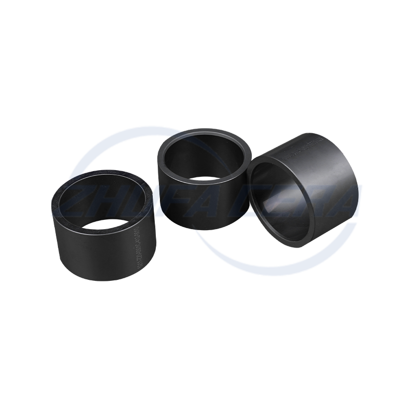
Black silicon carbide ceramic ring is a high-performance engineered ceramic assembly made of high-purity silicon carbide by precision molding and high temperature sintering. Its quadrangular crystal s...
See Details
FOLLOW US :


 Email: zf@zfcera.com
 Telephone: +86-188 8878 5188

Leading Precision Manufacturing | Key Applications of Advanced Precision Ceramics in Semiconductor Equipment
2026-04-11
In the microscopic world of semiconductor manufacturing, the evolution of nanoscale processes is not only a contest of photolithographic resolution, but also a secret battle of underlying material science. As chip manufacturing continues to advance toward 3nm and below processes, the process environment is undergoing extreme tests—ultra-high vacuum, highly corrosive plasma, and thermal stress sufficient to cause micron-level deformation.
In this context, traditional metal and organic materials are gradually withdrawing from the core technology stage due to limitations in their physical properties. Precision ceramic components have become an indispensable "rigid cornerstone" in semiconductor equipment due to their high hardness, high elastic modulus, corrosion resistance and excellent thermal stability. According to industry data, the value share of precision ceramic components in advanced semiconductor equipment has jumped to about 16%. This is no longer just a replacement of parts, but a material revolution related to the safety of the industrial chain and the upper limit of the process.
一、 从高纯氧化铝到功能性氮化物的跨越
半导体设备对陶瓷的需求并非单一维度,而是根据刻蚀、沉积、光刻等不同工序的物理边界,形成了以氧化铝、氮化铝、氧化锆等为核心的材料矩阵。
As the most widely used oxide ceramic, the core value of high-purity alumina lies in its "extreme chemical inertness". In the dry etching process, fluorine-based or chlorine-based plasma will produce strong chemical erosion of the cavity. High-purity alumina with a purity of more than 99.9% can not only resist plasma erosion by controlling the impurity content, but also effectively avoid secondary contamination of the wafer by metal ions. This material, which balances cost and performance, is widely used in gas nozzles, distribution plates and cavity linings.
However, when the process involves severe heat exchange, aluminum nitride shows irreplaceable advantages. As a nitride with both high thermal conductivity and excellent insulation properties, its thermal expansion coefficient surprisingly matches that of single crystal silicon. This match greatly reduces the risk of wafer edge warping due to thermal stress during processing of 12-inch wafers. At present, aluminum nitride has become a strategic material for manufacturing electrostatic chucks and high-performance heaters, which directly determines the upper limit of temperature uniformity in the process.
In addition, for downstream packaging and precision transmission links, zirconia stands out with its rare high toughness among ceramic systems. Through toughening processes such as yttrium stabilization, zirconia overcomes the natural fragility of ceramics, allowing it to withstand high-frequency vibration and physical impact when manufacturing precision ceramic cleavers, bearings and valves, significantly extending the mean time between failures of the equipment.
2. Support process empowerment throughout the life cycle
The application of precision ceramics is not an isolated replacement, but is deeply embedded in the entire life cycle of semiconductor manufacturing.
in Front etching link , As a key component to protect the edge of the wafer and correct the plasma flow field, the focus ring must maintain absolute stability in size under extreme environments. The focus ring made of precision ceramics can significantly reduce the frequency of replacement of consumables, thus improving the machine's availability.
in Lithography machine system Among them, precision ceramics are the "behind-the-scenes heroes" who pursue ultimate silence and precision. In order to achieve nanometer-level alignment accuracy, the workpiece stage of the photolithography machine requires extremely high specific stiffness and low thermal expansion coefficient. Guide rails, square mirrors and vacuum suction cups made of silicon carbide and silicon nitride ensure that during high-speed scanning movements, the system will not generate displacement offsets that are sufficient to affect yield due to tiny heat.
in Back-end packaging process , precision ceramics also play a key role. Taking wire bonding as an example, the wear resistance and anti-adhesion ability of the ceramic riving knife under high-speed operation are directly related to the reliability of the bonding wire. Zirconia-based ceramics ensure that every gold wire as thin as a hair can be accurately anchored due to its excellent surface roughness control and physical strength.
3. Technological breakthrough under the wave of localization
From a global perspective, the high-end market for precision ceramics has long been occupied by a few giants from Japan, the United States and Europe. However, with the in-depth adjustment of the global semiconductor industry chain, domestic precision ceramics are ushering in a golden period of transformation from "laboratory research and development" to "industrialization and mass production".
Upgrading of manufacturing processes: Domestic companies are gradually conquering the full-process technology from high-purity powder preparation to advanced molding. Especially in the field of large-size air pressure sintered silicon nitride ceramics, domestic technological breakthroughs have broken the long-term dependence on imports and achieved independent control of core components.
Bidirectional breakthroughs in size and precision: With the large-scale expansion of 12-inch wafer fabs, the demand for large-diameter, special-shaped ceramic parts has surged. Future technological competition will focus on how to ensure the uniform release of internal stress in large-size components and achieve nanoscale surface finishing through diamond grinding and laser microhole processing.
"Demetallization" and ultra-high purification: In order to cope with more advanced manufacturing processes, ceramic materials are moving towards "4N (99.99%)" or even higher purity. Reducing trace metal impurities within materials has become the only way to improve the yield of advanced process chips.
Promote the "advance" of the industry with the "refinement" of materials
Precision ceramics are not only components of semiconductor equipment, but also the material origin supporting the modern microelectronics industry. For equipment engineers, an in-depth understanding of the physical and chemical properties of ceramic materials is the basis for optimizing machine performance; for procurement decision-makers, establishing a stable and high-quality ceramic supply chain is the key to avoiding supply interruption risks and improving overall cost of ownership competitiveness.
As China's semiconductor-grade advanced ceramics market moves towards hundreds of billions, we are witnessing a leap from "material import" to "technology export".
[Professional consultation and technical support]
We have been deeply involved in the research and development of precision ceramics in the semiconductor field for many years, providing a full range of customized solutions including high-purity alumina, aluminum nitride, silicon nitride and zirconium oxide. If you are looking for ceramic components that can handle extreme working conditions, or would like to have an in-depth discussion on domestic alternatives, please contact our technical team.
Precision reaches far, ceramic core. We look forward to exploring the infinite possibilities of materials science with you.
Related products
-
-
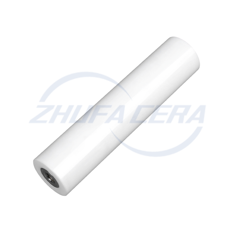
Zirconia Ceramic Rod is a high-performance ceramic material rod, mainly made of zirconium oxide, with excellent mechanical strength and chemical stability. It exhibits extremely high hardness and wear...
See Details -
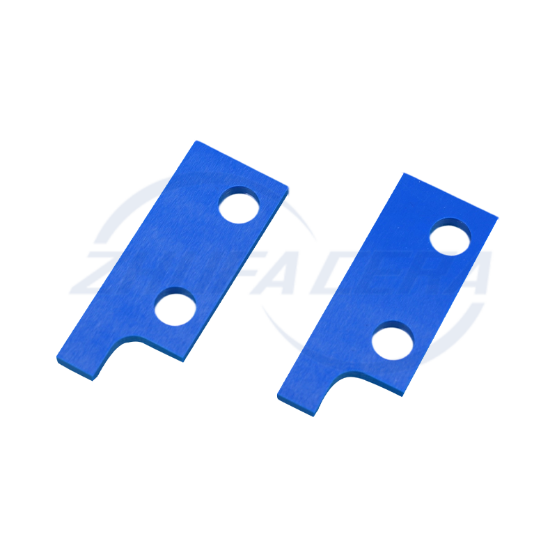
Blue zirconia ceramic sheets are precision components made of advanced zirconia ceramics. They are stained with cobalt, iron or copper to form a blue color. This color not only serves as a visual i...
See Details -

This blue zirconia ceramic pin is made of advanced zirconia ceramic material, providing excellent durability and performance. Zirconia ceramics are known for their high strength, good wear resistan...
See Details -

Zirconia Ceramic Gear is made of zirconium oxide ceramic material, which has excellent high strength and high hardness. This material property enables it to effectively resist wear during the transmis...
See Details -
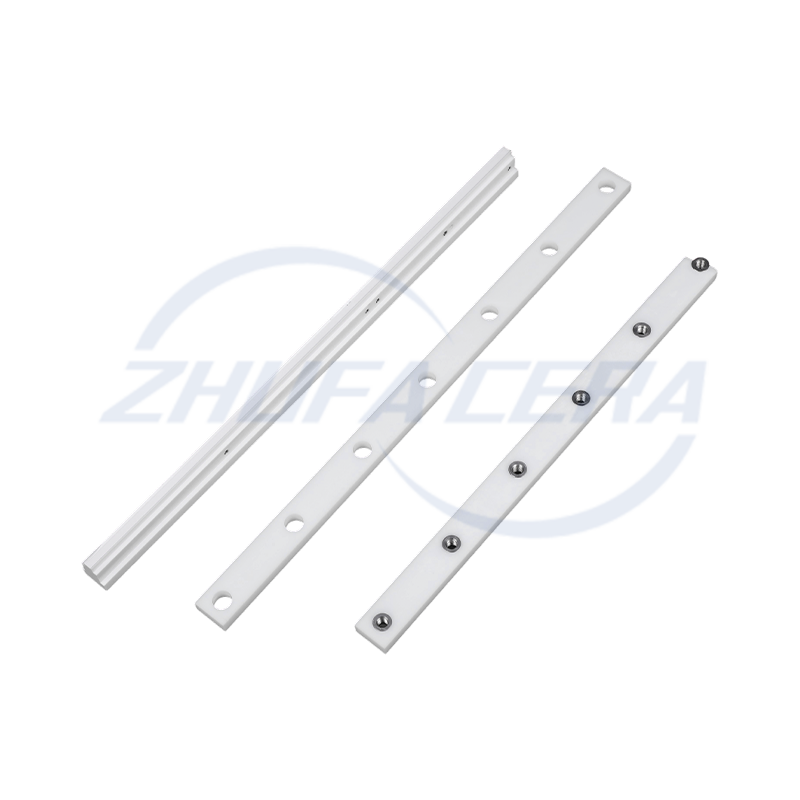
Zirconia Ceramic Guide Rail is a high-performance precision mechanical component made of zirconium oxide ceramic material. Its core characteristics are derived from the excellent physical and chemical...
See Details -
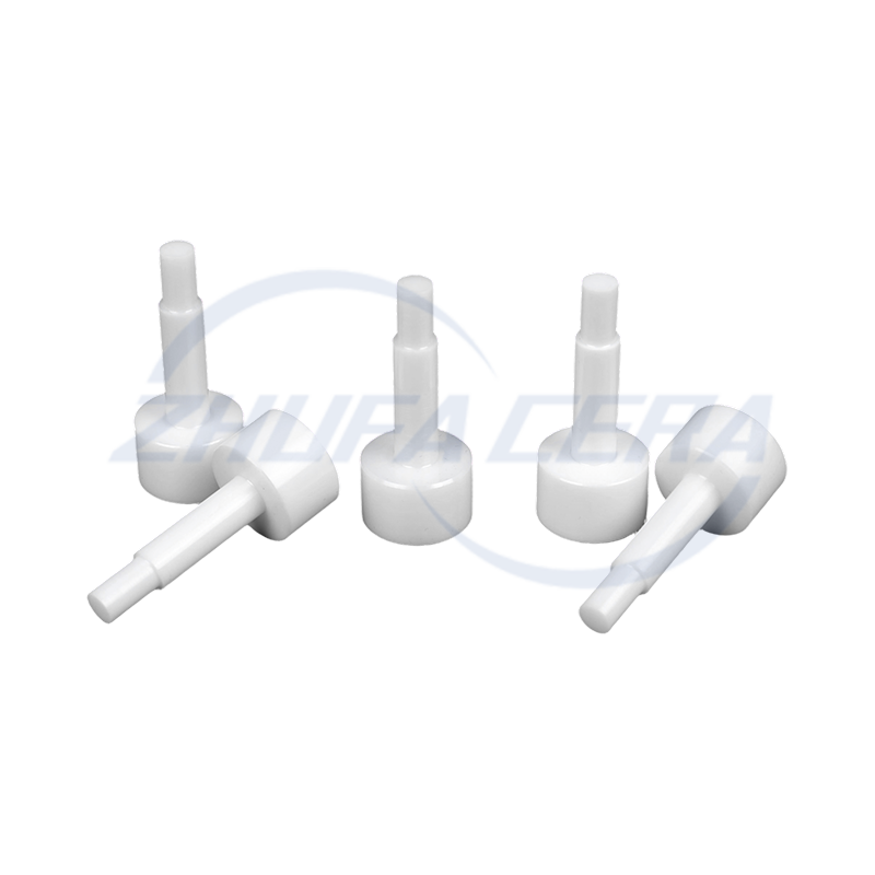
Zirconia Ceramic Locating Pin is a high-precision positioning element made of advanced zirconium oxide ceramic material with excellent physical and chemical properties. Its main characteristics includ...
See Details -
Zirconia Ceramic Ring is a high-performance ceramic product known for its excellent physical and chemical properties. It has extremely high hardness and strength, with a Mohs hardness of more than 8.5...
See Details -
Zirconia ceramic sheets have become functional core components in various fields thanks to their unique properties. With a flexural strength of 900–1200 MPa and a fracture toughness of 6–10 MPa・m¹/², ...
See Details -

Zirconia Ceramic Strip is a strip material made of high-performance zirconium oxide ceramic with excellent physical and chemical properties. It has extremely high hardness and flexural strength, can e...
See Details -
Zirconia ceramic wafers are representative products in the field of high-performance structural ceramics. Compared with traditional alumina ceramics or metal materials, its comprehensive performanc...
See Details -
Zirconia Ceramic Plunger is a high-performance component designed for harsh industrial environments. Compared with similar ceramic or metal plunger products, it stands out with its unique material adv...
See Details

-
Quick Links
Home Products About Us Services Technology News Contact Us -
Products
Ceramic Structural Parts Zirconia Ceramics Alumina Ceramics ZTA Ceramics Silicon Nitride Ceramics Silicon Carbide Ceramics Ceramic Injection Molded Parts -
About Us
Factory Tour Honor FAQ -
Contact info
+86-188 8878 5188zf@zfcera.comNo. 1, Xinggong Road, Anchang Industrial Park, Keqiao District, Shaoxing City, Zhejiang Province, China -
WhatsApp

Copyright © Zhejiang Zhufa Precision Ceramics Technology Co., Ltd. All Rights Reserved.
China precision ceramics manufacturer
wholesale precision ceramics supplier
