

 中文简体
中文简体 русский
 Español
 عربى
عربى Português
 日本語
日本語 한국어
한국어
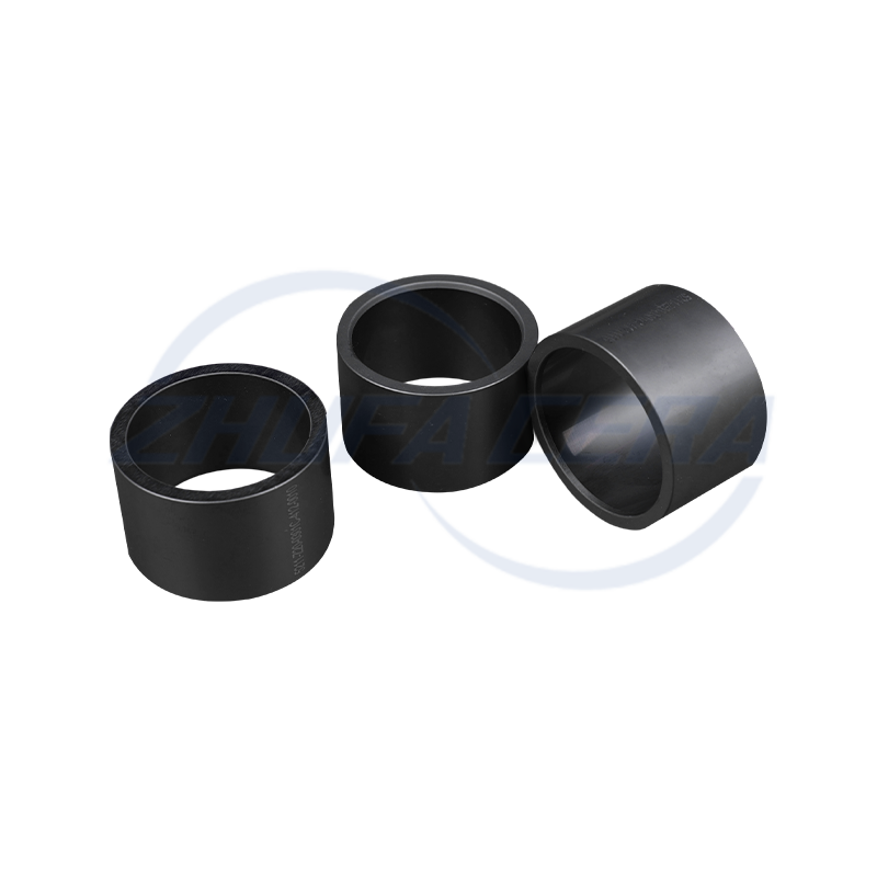
Black silicon carbide ceramic ring is a high-performance engineered ceramic assembly made of high-purity silicon carbide by precision molding and high temperature sintering. Its quadrangular crystal s...
See Details
FOLLOW US :


 Email: zf@zfcera.com
 Telephone: +86-188 8878 5188

Maximizing Yield in Semiconductor Plasma Etching: How Advanced Alumina Ceramic Chucks Eliminate Electrostatic and Particle Risks
2026-07-11
In modern semiconductor manufacturing, particularly as advanced nodes transition to 7nm, 5nm, and below, the tolerances for wafer defects have shrunk to near-zero. During the critical dry plasma etching process, wafers are exposed to extreme environments where electrostatic discharge (ESD) breakdowns, de-chucking delays, and particulate contamination pose catastrophic threats to device yield.
As the core insulating layer or high-precision substrate of Electrostatic Chucks (ESCs) and vacuum susceptors, Advanced Alumina (Al₂O₃) Ceramics have become irreplaceable. Through tailored material modification, microstructural engineering, and superior chemical resilience, advanced alumina ceramic chucks successfully neutralize these two industry-wide pain points.
————————————————————————————————————————
- Resolving the Dilemma: From "Ultra-Insulative" to "Electrostatic Dissipative"
Traditional high-purity alumina is celebrated for its excellent electrical insulation properties. However, inside a high-density plasma etching chamber, this classic benefit becomes a liability. Pure insulators accumulate massive amounts of surface static charges during processing. This leads to two critical failures:
- Excessive Residual Clamping Force: The wafer remains "dead-locked" to the chuck even after the voltage is turned off, causing wafer breakage or severe mechanical handling delays during de-chucking.
- Electrostatic Discharge (ESD): Accumulated localized charges can suddenly discharge, puncturing the delicate dielectric layers of the integrated circuits on the wafer.
To overcome this bottleneck, advanced semiconductor ceramic manufacturers utilize sophisticated material doping to transform pure alumina from an absolute insulator into a controlled semiconducting/electrostatic dissipative material.
Precision Volume Resistivity Control via Doping
By embedding trace amounts of transition metal oxides—such as Titanium Dioxide (TiO₂) or Chromium Oxide (Cr₂O₃)—into the alumina matrix, engineers can precisely tune the material’s bulk property. The goal is to tightly control its volume resistivity within the optimal electrostatic dissipative window, typically 10⁹ to 10¹¹ Ω·cm.
Furthermore, because etching processes run at varying temperatures, the doping chemistry must ensure a stable temperature coefficient of resistance (TCR). This prevents the chuck from losing its dissipative properties as the chamber heats up.
Harnessing the Johnsen-Rahbek (J-R) Effect for High-Speed De-Chucking
Unlike traditional Coulombic electrostatic chucks that require ultra-high voltages to generate holding force through perfect dielectrics, modified semiconductive alumina chucks primarily operate on the Johnsen-Rahbek (J-R) effect.
|
Technology |
Key Attributes & Operational Differences |
|
Coulombic Chuck |
Requires exceptionally high voltage. Demonstrates slower electrostatic charge release times and lower peak clamping force across varying gas pressures. |
|
J-R Effect Chuck |
Relies on micro-current migration. Produces a massive clamping force at lower voltages and achieves near-instant electrostatic charge release. |
When a DC bias voltage is applied, microscopic currents migrate through the semi-insulating alumina, concentrating charges at the microscopic asperities (crests) where the ceramic surface meets the wafer backside. Because the effective charge separation distance is reduced to a sub-micron scale, the resulting clamping force is several times stronger than pure Coulombic forces.
More importantly, the moment the power supply is cut or reversed, the semi-conductive pathways allow these accumulated charges to bleed away almost instantly. This achieves near-zero residual suction and completely eliminates wafer de-chucking delays, significantly boosting wafer-per-hour (WPH) throughput.
- Preventing Contamination: Ultra-High Purity and Micro-Structured Surface Engineering
The dry etching environment is inherently destructive. It relies on aggressive, highly corrosive halogenated fluorocarbon and chlorine gases (e.g., CF₄, CHF₃, Cl₂, BCl₃) paired with intense, directional RF-driven ion bombardment. If the ceramic substrate lacks sufficient mechanical and chemical durability, it will erode over time, shedding lethal sub-micron particles onto the wafer.
To achieve a "zero-contamination" standard in front-end wafer fabrication, advanced alumina components undergo strict multi-dimensional engineering.
Ultra-High Purity Raw Materials (99.5% to 99.99%)
Alumina materials designated for front-end semiconductor processing must restrict trace metal impurities to absolute minimums. Critical mobile ions such as Copper (Cu), Iron (Fe), Sodium (Na), and Potassium (K) are strictly capped at low ppm (parts per million) or even ppb (parts per billion) thresholds.
If these metals were to leach out due to gradual ceramic wear, they would diffuse into the silicon substrate, causing deep-level contamination, altering threshold voltages, and leading to irreversible device short-circuits.
Superior Plasma and Chemical Erosion Resistance
High-purity alumina ceramics possess exceptionally high lattice energy and chemical stability. When subjected to continuous reactive ion etching (RIE), the chemical erosion rate remains exceptionally low. The dense, fine-grained microstructure—typically achieved through advanced Cold Isostatic Pressing (CIP) and optimized vacuum sintering profiles—ensures that the grain boundaries do not etch preferentially, preventing the dislodgement of entire ceramic grains (particle shedding).
Precision "Mesa" (Micro-Bumper) Surface Design
Even with high-purity materials, direct friction between a flat ceramic surface and a silicon wafer can generate mechanical particles. To circumvent this, the contact surface of advanced alumina chucks is never entirely flat. Instead, it is patterned with engineered micro-structures known as Mesas or Micro-Bumpers.
- >90% Contact Area Reduction: The micro-mesa pattern reduces the actual physical contact area between the chuck and the wafer backside by more than 90%. This drastically lowers the probability of mechanical friction-induced particle generation.
- Particle Trapping Cavities: The valleys and grooves between these micro-mesas serve a dual purpose. They act as flow channels for Helium (He) backside cooling gas and double as protective pockets. If any stray particles are generated, they gravitate safely into these recessed grooves, preventing them from pressing against the wafer backside.
Technical Summary: The Strategic Integration of "Grit and Grace"
In the tempest of semiconductor plasma etching, advanced alumina ceramic chucks serve as a masterpiece of industrial material design. By masterfully adjusting electrical properties, they allow electrostatic charges to gather with immense force and dissipate in milliseconds, overcoming the challenge of residual sticking. Simultaneously, through ultra-pure compositions and engineered micro-surfaces, they stand resilient against violent plasma bombardment—safeguarding semiconductor wafers from both particulate and metallic contamination.
For tier-1 semiconductor OEMs and wafer fabs, investing in precisely modified, ultra-pure alumina components is not just a material choice; it is a fundamental strategy for maximizing tool uptime and securing consistent wafer yield.
Related products
-
-
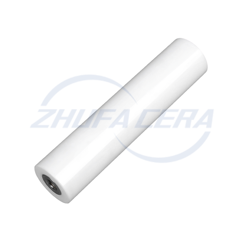
Zirconia Ceramic Rod is a high-performance ceramic material rod, mainly made of zirconium oxide, with excellent mechanical strength and chemical stability. It exhibits extremely high hardness and wear...
See Details -
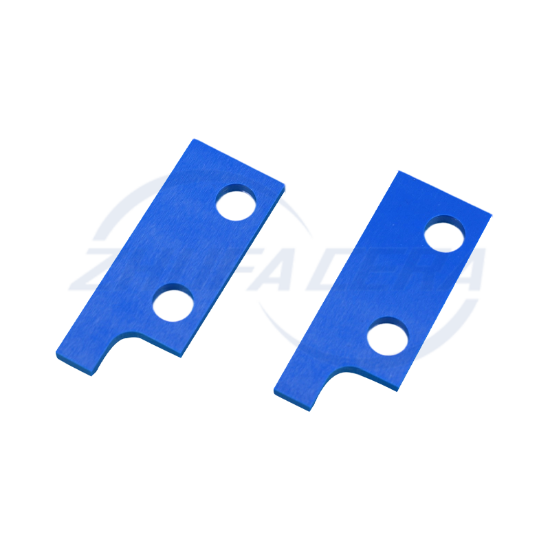
Blue zirconia ceramic sheets are precision components made of advanced zirconia ceramics. They are stained with cobalt, iron or copper to form a blue color. This color not only serves as a visual i...
See Details -
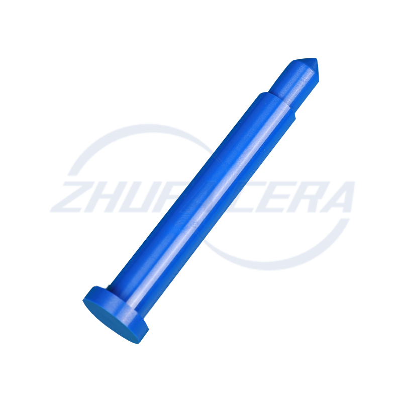
This blue zirconia ceramic pin is made of advanced zirconia ceramic material, providing excellent durability and performance. Zirconia ceramics are known for their high strength, good wear resistan...
See Details -

Zirconia Ceramic Gear is made of zirconium oxide ceramic material, which has excellent high strength and high hardness. This material property enables it to effectively resist wear during the transmis...
See Details -
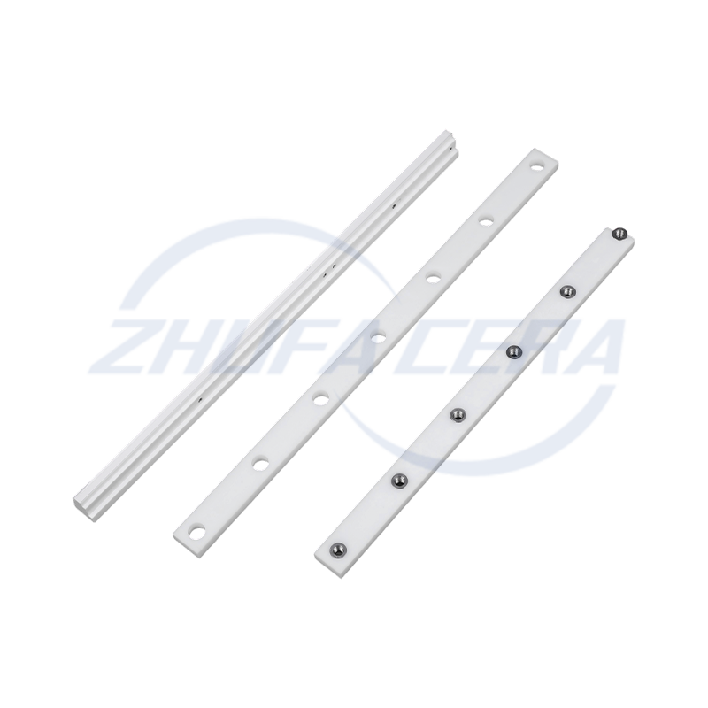
Zirconia Ceramic Guide Rail is a high-performance precision mechanical component made of zirconium oxide ceramic material. Its core characteristics are derived from the excellent physical and chemical...
See Details -
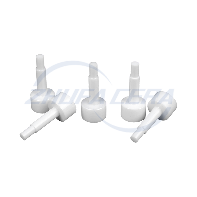
Zirconia Ceramic Locating Pin is a high-precision positioning element made of advanced zirconium oxide ceramic material with excellent physical and chemical properties. Its main characteristics includ...
See Details -
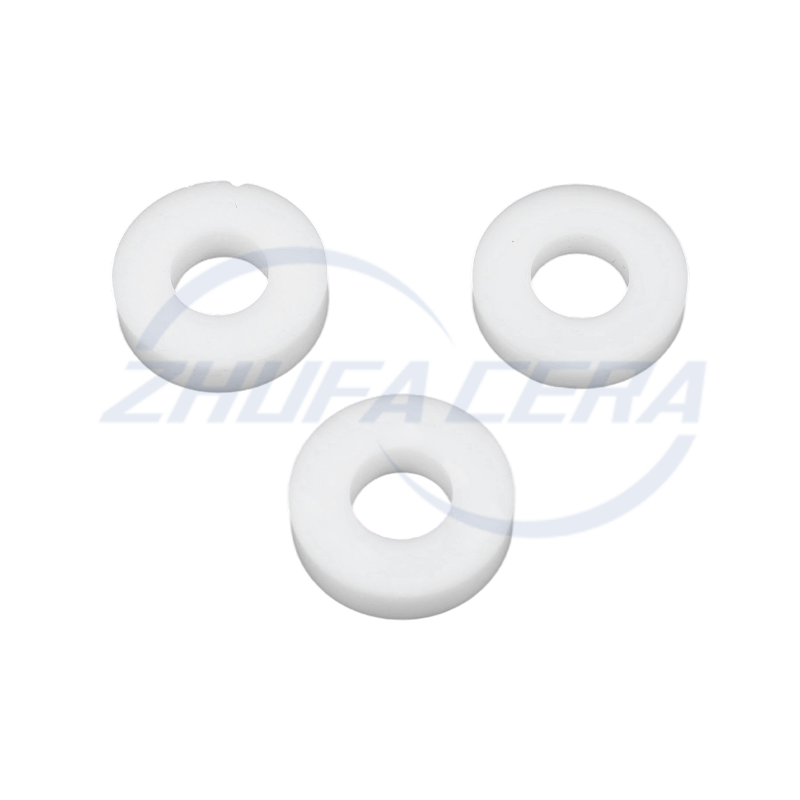
Zirconia Ceramic Ring is a high-performance ceramic product known for its excellent physical and chemical properties. It has extremely high hardness and strength, with a Mohs hardness of more than 8.5...
See Details -
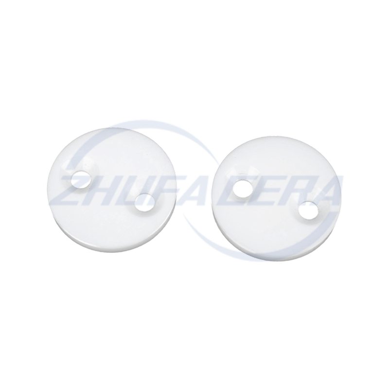
Zirconia ceramic sheets have become functional core components in various fields thanks to their unique properties. With a flexural strength of 900–1200 MPa and a fracture toughness of 6–10 MPa・m¹/², ...
See Details -

Zirconia Ceramic Strip is a strip material made of high-performance zirconium oxide ceramic with excellent physical and chemical properties. It has extremely high hardness and flexural strength, can e...
See Details -
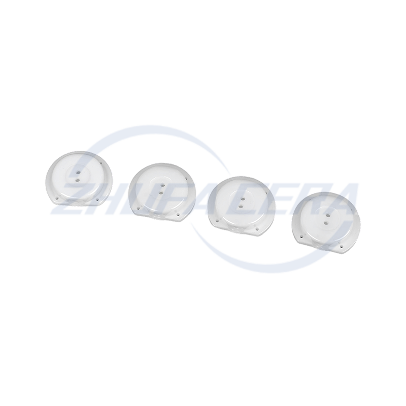
Zirconia ceramic wafers are representative products in the field of high-performance structural ceramics. Compared with traditional alumina ceramics or metal materials, its comprehensive performanc...
See Details -
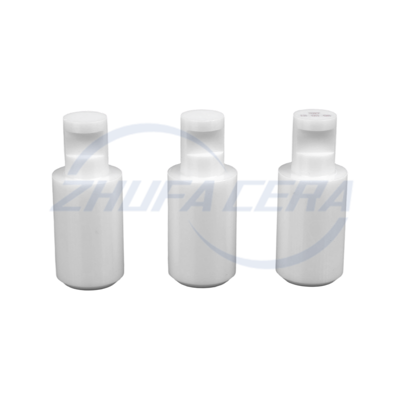
Zirconia Ceramic Plunger is a high-performance component designed for harsh industrial environments. Compared with similar ceramic or metal plunger products, it stands out with its unique material adv...
See Details


-
Quick Links
Home Products About Us Services Technology News Contact Us -
Products
Ceramic Structural Parts Zirconia Ceramics Alumina Ceramics ZTA Ceramics Silicon Nitride Ceramics Silicon Carbide Ceramics Ceramic Injection Molded Parts -
About Us
Factory Tour Honor FAQ -
Contact info
+86-188 8878 5188zf@zfcera.comNo. 1, Xinggong Road, Anchang Industrial Park, Keqiao District, Shaoxing City, Zhejiang Province, China -
WhatsApp

Copyright © Zhejiang Zhufa Precision Ceramics Technology Co., Ltd. All Rights Reserved.
China precision ceramics manufacturer
wholesale precision ceramics supplier
