

 中文简体
中文简体 русский
 Español
 عربى
عربى Português
 日本語
日本語 한국어
한국어
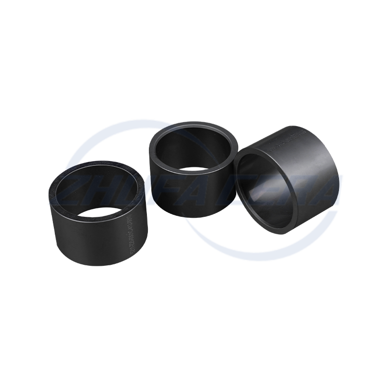
Black silicon carbide ceramic ring is a high-performance engineered ceramic assembly made of high-purity silicon carbide by precision molding and high temperature sintering. Its quadrangular crystal s...
See Details
FOLLOW US :


 Email: zf@zfcera.com
 Telephone: +86-188 8878 5188

Ceramic Vacuum Chucks vs. Electrostatic Chucks (ESC) in Semiconductor Manufacturing
2026-06-30
In the highly precise realm of semiconductor front-end manufacturing, every single wafer must undergo hundreds of complex, rigorous steps—cycling through extreme thermal transitions, high-pressure vacuums, and intense plasma bombardment. Within this micro- and nano-scale technological odyssey, securely, accurately, and flawlessly holding the wafer becomes a paramount determinant of ultimate chip yield.
In this domain, Ceramic Vacuum Chucks and Electrostatic Chucks (ESC) are undoubtedly the two foundational holding technologies. Industry newcomers often ask: 'Since both are made of advanced ceramics and both hold wafers, why is there a multi-order-of-magnitude price difference? What sets them apart?' Today, we will demystify these two advanced solutions, dissect their core differences, and guide you on choosing the ideal technology for your specific process.
- Ceramic Vacuum Chucks: The Heavy-Lifter of Atmospheric Environments
The operational logic of the ceramic vacuum chuck aligns closely with intuitive physical mechanics: pressure differential.
- Working Principle: The surface is typically engineered from high-purity porous ceramics (such as Alumina, Al₂O₃, or Silicon Carbide, SiC), embedded with countless micron-sized microscopic pores. When the equipment evacuates air between the chuck and the wafer, a negative pressure zone forms inside. Consequently, ambient atmospheric pressure acts as an invisible force, firmly pressing the wafer against the chuck surface.
- Key Advantages: Ceramic vacuum chucks feature exceptional hardness and wear resistance. Their rigid mechanical structure delivers immense stability during high-speed machining. Furthermore, their straightforward architecture ensures high cost-effectiveness, simple deployment, and straightforward maintenance.
- Inherent Limitations: They suffer from a critical limitation—vacuum vulnerability. Because they rely entirely on ambient atmospheric pressure differentials, they lose their holding force instantly when placed inside a high-vacuum chamber where no external air pressure exists.
- Electrostatic Chucks (ESC): The Vacuum and Plasma Specialist
When a process migrates to high vacuum, ultra-high vacuum, or intense plasma environments, standard vacuum chucks become completely non-functional. For these demanding front-end environments, semiconductor tools must utilize high-value Electrostatic Chucks (ESC).
- Working Principle: An ESC features a highly complex network of embedded micro-electrodes within its ceramic body. Applying high-voltage direct current (DC) induces opposite electrical charges between the electrodes and the wafer, generating a robust Coulombic or Johnsen-Rahbek electrostatic force. This electromagnetic field clamps the wafer perfectly flat without any physical atmospheric dependence.
- Vacuum Immunity: Operating seamlessly without any gaseous ambient media, maintaining strong, reliable clamping forces even in ultra-high vacuum environments.
- Extreme Uniformity and Flatness: The electrostatic clamping force is distributed uniformly across the entire surface of the wafer. This minimizes localized stress concentrations and eliminates substrate deformation, resulting in exceptional sub-nanometer flatness.
- Advanced Thermal Control: Thermal dissipation is exceptionally difficult in a vacuum environment. ESC systems mitigate this by integrating a complex, backside Helium (He) gas cooling channel network. This architecture allows the chuck to regulate wafer temperatures with extreme precision—often within ±1°C—even under intense plasma heat loads.
- Core Differences at a Glance
|
Feature Dimension |
Ceramic Vacuum Chuck |
Electrostatic Chuck (ESC) |
|
Clamping Force Source |
External atmospheric pressure differential (via vacuum pump negative pressure) |
Internal high-voltage electrostatic field generating Coulombic / Johnsen-Rahbek forces |
|
Primary Application Arena |
Atmospheric or low-vacuum environments (e.g., thinning, dicing, photoresist coating) |
High-vacuum / plasma-enhanced environments (e.g., Etch, PVD, CVD, Ion Implantation) |
|
Processing Precision |
Micron-level; susceptible to pore distribution limits and micro-particle stress localization |
Nanometer-level; completely uniform full-surface clamping for superior flatness |
|
Thermal Control Capacity |
Standard; lacks dynamic, high-efficiency active thermal dissipation in vacuum environments |
Exceptional; features multi-zone backside Helium (He) cooling channels for precise temperature tuning |
|
Capital Cost & Barrier |
Moderate cost, highly mature manufacturing process, straightforward integration |
Extremely expensive, highly proprietary multi-layer ceramic co-firing processes, severe technical barriers |
- Process Alignment Strategy: How to Choose?
The selection boundary between these two clamping solutions is distinct and driven entirely by your specific ambient environment:
- For Ambient & Post-Processing Operations: If your applications are focused on peripheral or back-end operations—such as wafer thinning, grinding, edge profiling, photoresist spin-coating, or automated optical inspection (AOI) within normal atmospheric environments—the Ceramic Vacuum Chuckrepresents the ideal choice. It offers unparalleled structural wear resistance, rigidity, and superior return-on-investment (ROI).
- For Core Front-End Lithography & Chamber Processing: If your process steps involve core sub-micron front-end operations—such as reactive-ion etching (RIE/ICP), physical vapor deposition (PVD), chemical vapor deposition (CVD), or high-dose ion implantation—the Electrostatic Chuck (ESC)is absolutely irreplaceable. It is the only choice capable of enduring deep vacuums, managing high-energy plasma thermal shifts, and maintaining precise substrate morphology.
Conclusion
Whether it is the robust, cost-effective ceramic vacuum chuck that excels under normal atmospheric conditions, or the high-tech, intricately engineered Electrostatic Chuck (ESC) designed for vacuum environments, both are vital pillars of modern semiconductor toolsets. Aligning your hardware choices with your precise chemical and atmospheric environment is paramount to boosting equipment uptime and overall yield.
|
Need Professional Clamping Support? If you are currently designing or optimizing advanced semiconductor tools, looking for tailored wafer-holding solutions, or evaluating ceramic material specifications for demanding thermal/chemical applications, please contact our technical engineering team for deep architectural consultation, material data sheets, and custom manufacturing solutions. |
Related products
-
-
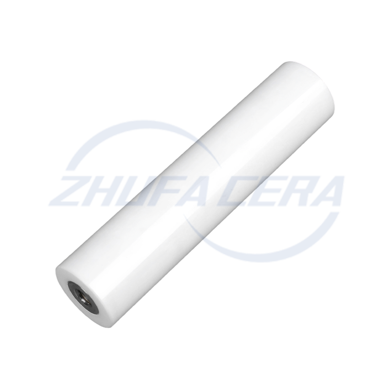
Zirconia Ceramic Rod is a high-performance ceramic material rod, mainly made of zirconium oxide, with excellent mechanical strength and chemical stability. It exhibits extremely high hardness and wear...
See Details -
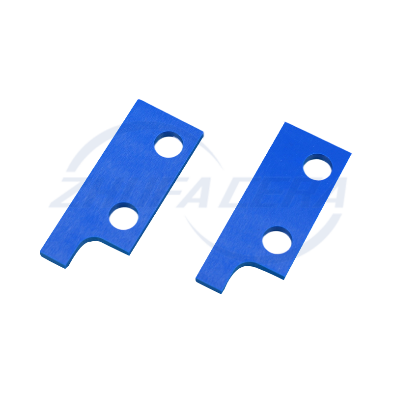
Blue zirconia ceramic sheets are precision components made of advanced zirconia ceramics. They are stained with cobalt, iron or copper to form a blue color. This color not only serves as a visual i...
See Details -
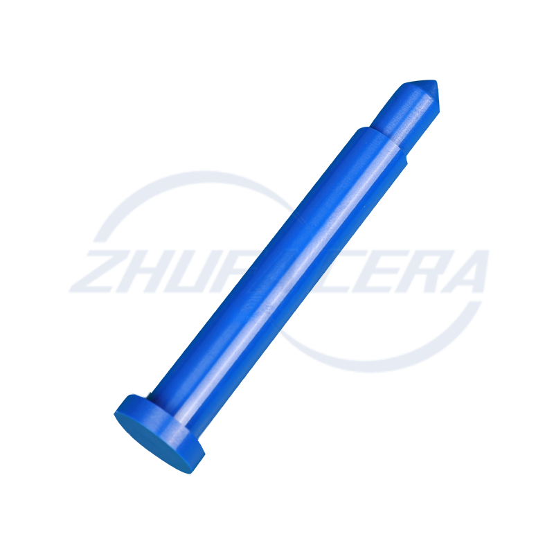
This blue zirconia ceramic pin is made of advanced zirconia ceramic material, providing excellent durability and performance. Zirconia ceramics are known for their high strength, good wear resistan...
See Details -

Zirconia Ceramic Gear is made of zirconium oxide ceramic material, which has excellent high strength and high hardness. This material property enables it to effectively resist wear during the transmis...
See Details -
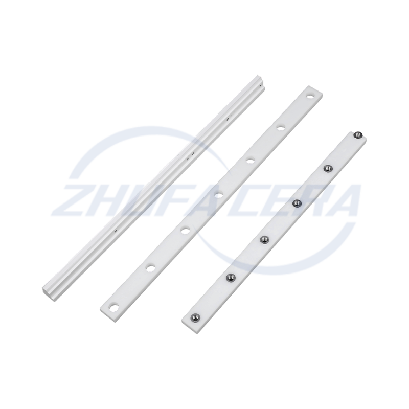
Zirconia Ceramic Guide Rail is a high-performance precision mechanical component made of zirconium oxide ceramic material. Its core characteristics are derived from the excellent physical and chemical...
See Details -
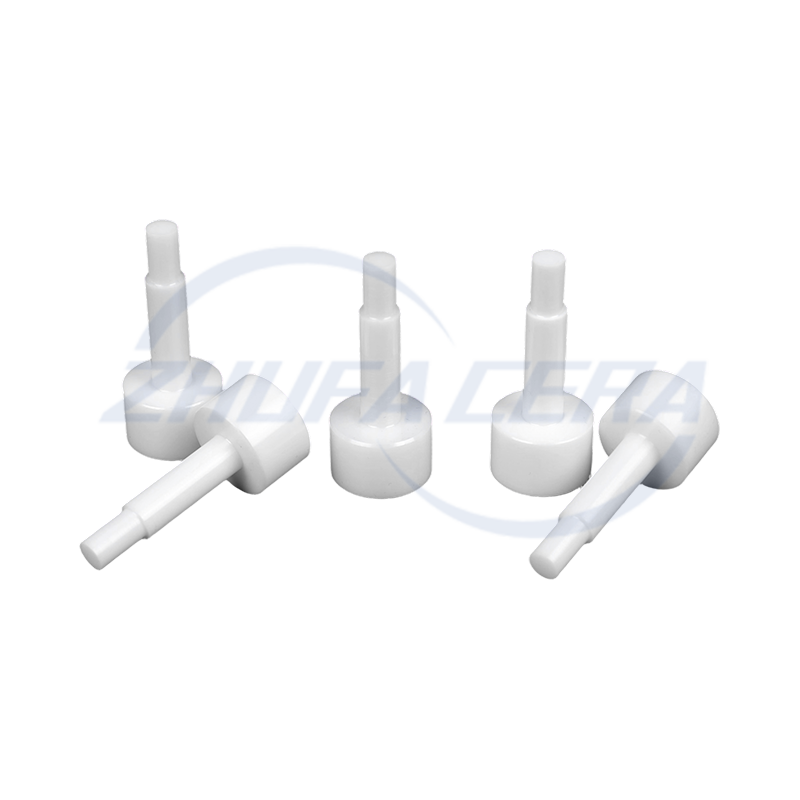
Zirconia Ceramic Locating Pin is a high-precision positioning element made of advanced zirconium oxide ceramic material with excellent physical and chemical properties. Its main characteristics includ...
See Details -
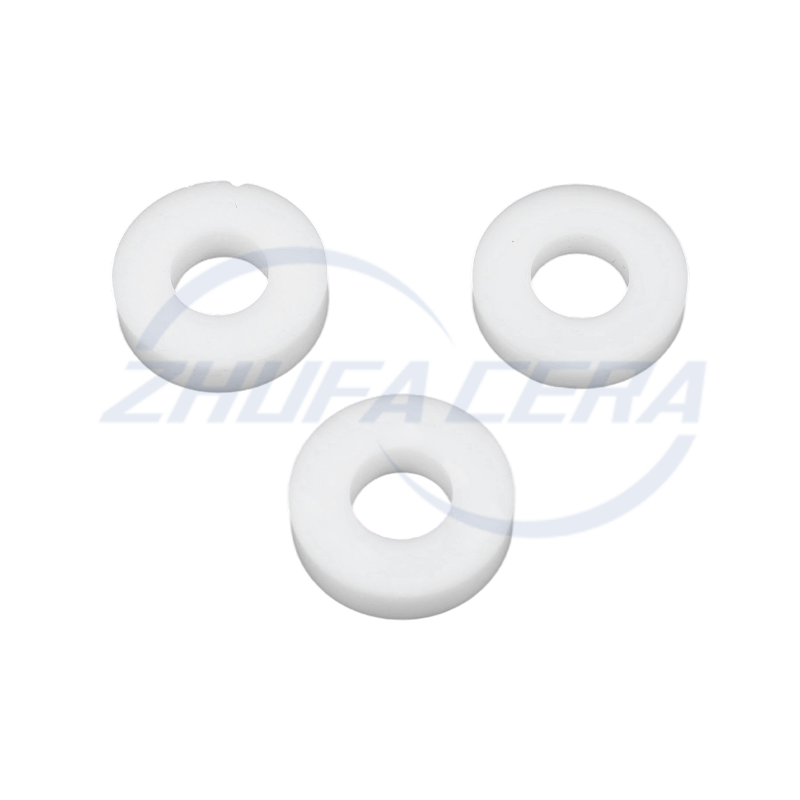
Zirconia Ceramic Ring is a high-performance ceramic product known for its excellent physical and chemical properties. It has extremely high hardness and strength, with a Mohs hardness of more than 8.5...
See Details -
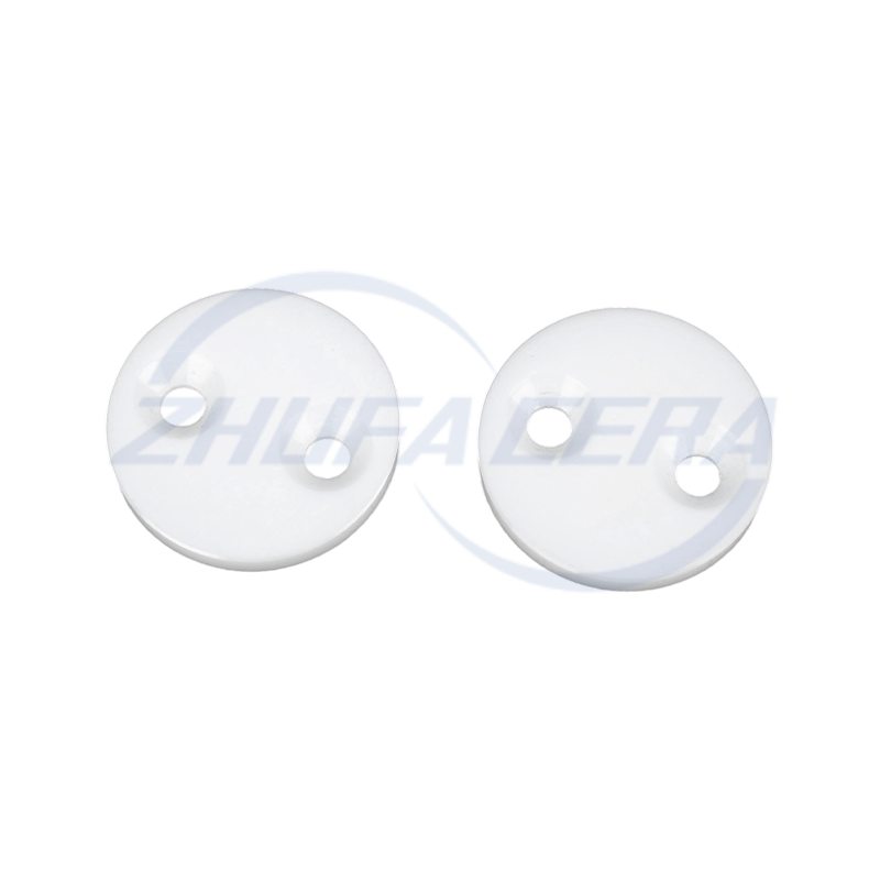
Zirconia ceramic sheets have become functional core components in various fields thanks to their unique properties. With a flexural strength of 900–1200 MPa and a fracture toughness of 6–10 MPa・m¹/², ...
See Details -

Zirconia Ceramic Strip is a strip material made of high-performance zirconium oxide ceramic with excellent physical and chemical properties. It has extremely high hardness and flexural strength, can e...
See Details -
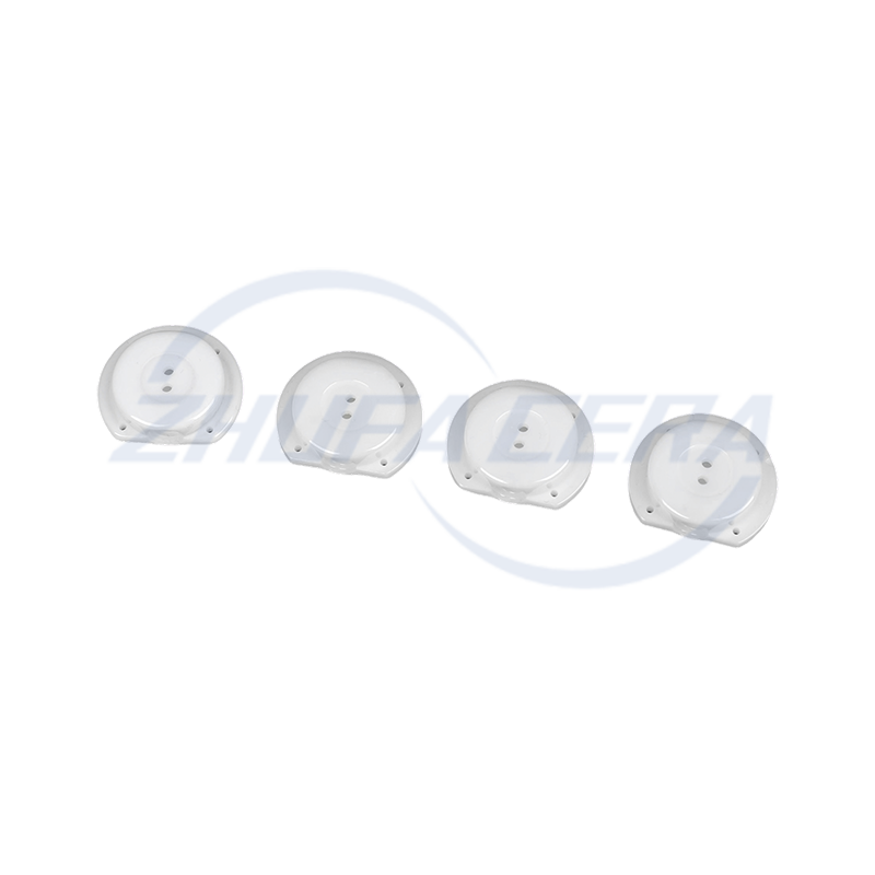
Zirconia ceramic wafers are representative products in the field of high-performance structural ceramics. Compared with traditional alumina ceramics or metal materials, its comprehensive performanc...
See Details -
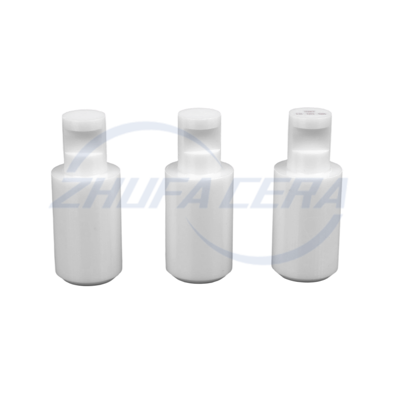
Zirconia Ceramic Plunger is a high-performance component designed for harsh industrial environments. Compared with similar ceramic or metal plunger products, it stands out with its unique material adv...
See Details


-
Quick Links
Home Products About Us Services Technology News Contact Us -
Products
Ceramic Structural Parts Zirconia Ceramics Alumina Ceramics ZTA Ceramics Silicon Nitride Ceramics Silicon Carbide Ceramics Ceramic Injection Molded Parts -
About Us
Factory Tour Honor FAQ -
Contact info
+86-188 8878 5188zf@zfcera.comNo. 1, Xinggong Road, Anchang Industrial Park, Keqiao District, Shaoxing City, Zhejiang Province, China -
WhatsApp

Copyright © Zhejiang Zhufa Precision Ceramics Technology Co., Ltd. All Rights Reserved.
China precision ceramics manufacturer
wholesale precision ceramics supplier
