

 中文简体
中文简体 русский
 Español
 عربى
عربى Português
 日本語
日本語 한국어
한국어
Black silicon carbide ceramic ring is a high-performance engineered ceramic assembly made of high-purity silicon carbide by precision molding and high temperature sintering. Its quadrangular crystal s...
See Details
FOLLOW US :


 Email: zf@zfcera.com
 Telephone: +86-188 8878 5188

Microstructure vs. Ultra-High Vacuum: How Ceramic Grain Size Dictates Outgassing in Sub-2nm Lithography
2026-07-15
In the relentless march of semiconductor manufacturing toward sub-2nm nodes, every incremental process shrink demands a corresponding push to the absolute physical limits of material science. As lithography, etching, and thin-film deposition scale down to atomic dimensions, wafer processing has transitioned entirely into the realm of Ultra-High Vacuum (UHV, pressure less than 10⁻⁵ Pa).
In this absolute domain where even a single stray gas molecule is classed as a critical yield-killing contaminant, advanced technical ceramics—specifically high-purity Alumina (Al₂O₃), Silicon Carbide (SiC), and Aluminum Nitride (AlN)—have become indispensable. Because of their exceptional thermal stability, plasma erosion resistance, and structural rigidity, they are the materials of choice for wafer stages, electrostatic chucks (ESCs), and gas distribution showerheads.
However, beneath the seemingly impenetrable surface of these solid structural ceramics lies a silent, microscopic vulnerability that threatens vacuum integrity: outgassing. The outcome of this battle for vacuum purity is determined by a structural variable invisible to the naked eye: the grain size of the ceramic material.
- Grain Boundaries: The High-Speed Highways for Gas Molecules
To understand how grain size dictates outgassing rates, we must look at the ceramic's polycrystalline microstructure. Polycrystalline ceramics are not single, continuous crystals; they are dense agglomerations of microscopic single-crystal grains packed and bound together. The interfaces where these grains meet are called grain boundaries.
At the microscopic level, the migration of gas molecules trapped inside a ceramic component relies on diffusion. While the atoms inside a single grain are arranged in a highly ordered, tightly packed lattice, the grain boundaries are highly disordered. They are saturated with lattice defects, vacancies, and micro-voids.
Consequently, grain boundaries exhibit much higher localized energy states, acting as low-resistance paths for gas diffusion—essentially "high-speed highways" compared to the highly resistive bulk crystal lattice.
|
[Gas Inside Grain] |
When a ceramic has a fine grain size, the number of individual grains per unit volume increases exponentially. This dramatically escalates the grain boundary density (total grain boundary surface area per unit volume).
- Fine-Grained Ceramics: The dense, interconnected network of grain boundaries allows residual gases—such as hydrogen and carbon monoxide trapped during sintering, or moisture absorbed from the air—to migrate rapidly to the surface, resulting in a sustained and elevated outgassing rate in vacuum chambers.
- Coarse-Grained / Single-Crystal Materials: With grain boundaries severely reduced or entirely eliminated (such as in single-crystal sapphire), gas molecules are locked within the tight crystal lattice. They must rely on bulk volume diffusion (Dv), which is orders of magnitude slower than grain boundary diffusion (Dgb). As a result, the outgassing rate is suppressed to near-zero levels.
- Specific Surface Area and Geometric Adsorption Traps
Beyond internal diffusion dynamics, grain size directly determines the effective surface area (specific surface area) and micro-topography of the finished ceramic component. Even after nanometer-level mechanical polishing, the surface of a fine-grained ceramic exposed to vacuum is structurally composed of the exposed tips of countless microscopic grains. This micro-roughness yields a much higher microscopic specific surface area than coarse-grained equivalents.
Physical and Chemical Adsorption
When ceramic components are stored, handled, or machined in ambient atmosphere, this expanded surface area acts like a microscopic sponge, physically and chemically bonding with water molecules (H₂O) and airborne organics.
Energy Traps and Desorption Tail
Once inside a UHV chamber, the gas molecules trapped inside these microscopic grain boundary crevices find themselves in stable, low-energy potential wells. They do not release immediately during the initial pump-down phase. Instead, they desorb slowly and continuously when stimulated by thermal fluctuations during wafer exposure or plasma bombardment. This causes a phenomenon known as desorption lag (or outgassing tail), leading to chronic vacuum drift and unstable process conditions.
- The Triad of Densification, Closed Porosity, and Outgassing
In advanced ceramic processing, grain size, sintering dynamics, and porosity form a deeply interconnected triad. Fine ceramic powders possess high surface energy, which serves as a powerful thermodynamic driving force to promote rapid densification during sintering.
However, if the sintering parameters (temperature, pressure, and atmosphere) are not perfectly controlled, fine-grained ceramics are prone to trapping localized gases, leading to closed porosity within the microstructural matrix.
|
The Vacuum Crisis of Closed Pores |
- The Engineering Trade-off: Mechanical Strength vs. Vacuum Integrity
Given that coarse-grained or single-crystal ceramics exhibit such superior low-outgassing properties, why not use them exclusively? This is where the demanding reality of semiconductor hardware engineering forces a critical compromise.
According to the classical Hall-Petch relationship in materials mechanics, the yield strength (σ_y) of a material is inversely proportional to the square root of its average grain diameter (d):
σ_y = σ_0 + k_y / √d
Where σ_0 is the starting material's resistance to dislocation movement, k_y is the strengthening coefficient (a material-specific constant), and d is the average grain size. This formula highlights a fundamental conflict:
- Fine-Grained Ceramics (Smaller d): Offer exceptional mechanical strength, hardness, fracture toughness, and thermal shock resistance. This high mechanical performance is vital for structural components like wafer stages, which must undergo high-speed, high-acceleration maneuvers with sub-micron precision.
- Coarse-Grained Ceramics (Larger d): Excellent for minimizing vacuum outgassing, but their mechanical properties are compromised. They are highly susceptible to grain pull-out along grain boundaries during precision machining or under cyclic thermal stresses. This creates physical particle contaminants that ruin wafer yield.
- Advanced Engineering Solutions: Bridging the Divide
To achieve the elusive balance of high mechanical strength (fine grain structure) and low outgassing (coarse grain properties), advanced ceramic manufacturers deploy specialized microstructural modification and post-processing treatments:
|
Engineering Method |
Microstructural Mechanism |
Primary Objective |
|
High-Temperature Liquid Phase Sintering (LPS) |
Introduces trace glass-phase additives that segregate to the grain boundaries of fine grains, creating a dense, amorphous barrier layer. |
Blocks Grain Boundary Diffusion: |
|
Atomic Layer Deposition (ALD) Coating |
Deposits a conformal, atomic-scale oxide barrier layer (such as Al₂O₃ or Y₂O₃) across the polished ceramic surface. |
Surface Passivation: |
|
UHV Thermal Pre-Baking |
Subjecting completed ceramic components to prolonged, high-temperature thermal baking (typically 200°C to 400°C) inside dedicated ultra-high vacuum chambers. |
Controlled Outgassing: |
Conclusion
At the sub-2nm node, macro-scale semiconductor yields are ultimately decided by the micro-scale control of materials. The engineering debate surrounding advanced ceramic grain size is a prime example of this reality.
Understanding, modeling, and controlling the relationship between grain size, grain boundary chemistry, and UHV outgassing rates is no longer just an academic exercise—it is a core engineering pillar of the modern semiconductor industry. In the race to the physical limits of silicon, those who master microstructural control hold the key to vacuum process stability.
Related products
-
-
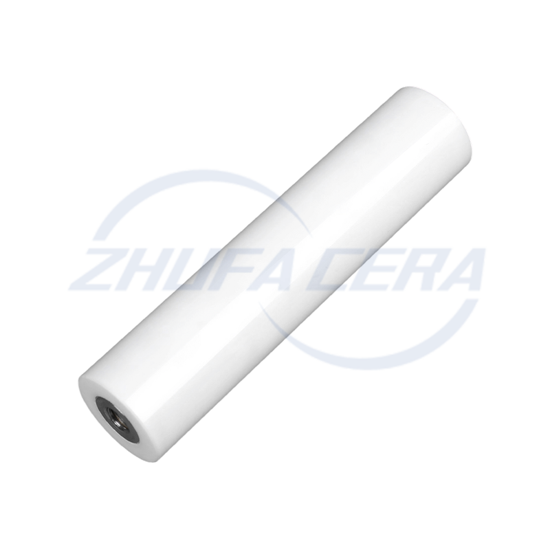
Zirconia Ceramic Rod is a high-performance ceramic material rod, mainly made of zirconium oxide, with excellent mechanical strength and chemical stability. It exhibits extremely high hardness and wear...
See Details -
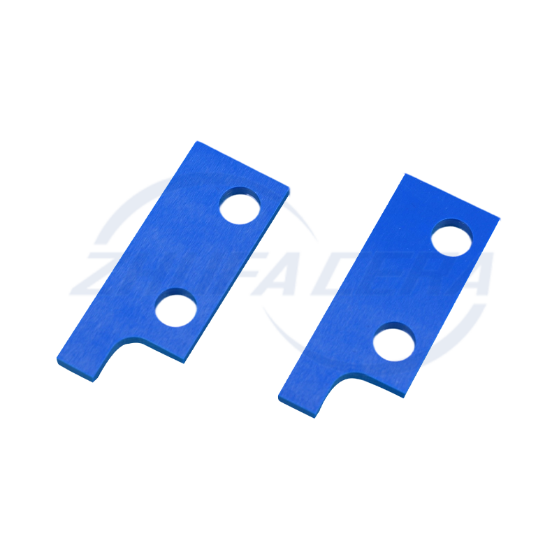
Blue zirconia ceramic sheets are precision components made of advanced zirconia ceramics. They are stained with cobalt, iron or copper to form a blue color. This color not only serves as a visual i...
See Details -

This blue zirconia ceramic pin is made of advanced zirconia ceramic material, providing excellent durability and performance. Zirconia ceramics are known for their high strength, good wear resistan...
See Details -

Zirconia Ceramic Gear is made of zirconium oxide ceramic material, which has excellent high strength and high hardness. This material property enables it to effectively resist wear during the transmis...
See Details -
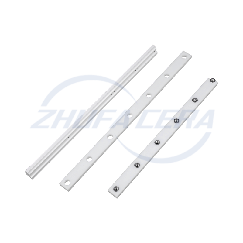
Zirconia Ceramic Guide Rail is a high-performance precision mechanical component made of zirconium oxide ceramic material. Its core characteristics are derived from the excellent physical and chemical...
See Details -
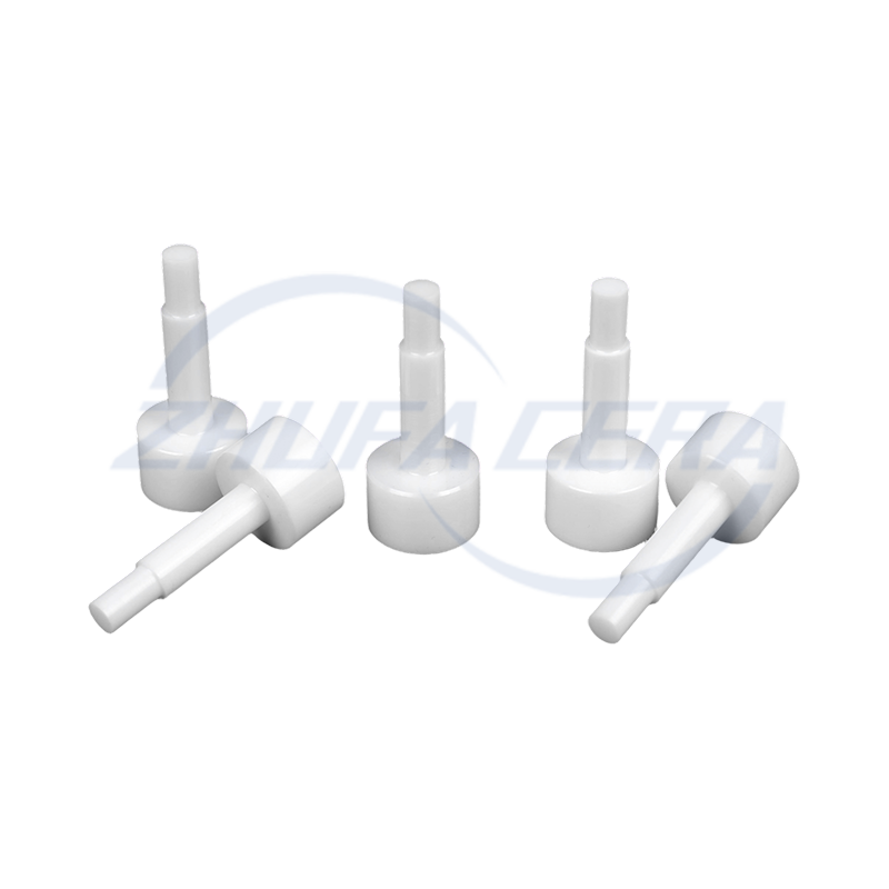
Zirconia Ceramic Locating Pin is a high-precision positioning element made of advanced zirconium oxide ceramic material with excellent physical and chemical properties. Its main characteristics includ...
See Details -

Zirconia Ceramic Ring is a high-performance ceramic product known for its excellent physical and chemical properties. It has extremely high hardness and strength, with a Mohs hardness of more than 8.5...
See Details -
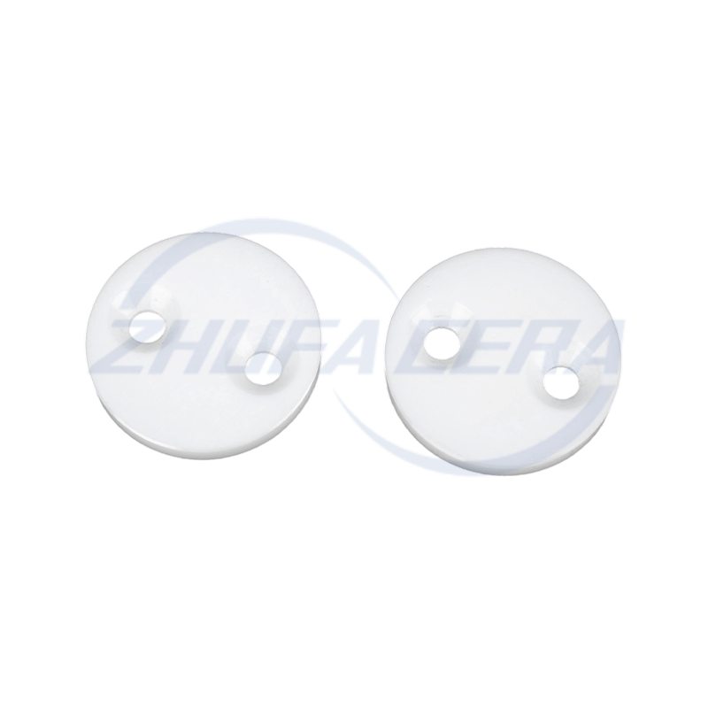
Zirconia ceramic sheets have become functional core components in various fields thanks to their unique properties. With a flexural strength of 900–1200 MPa and a fracture toughness of 6–10 MPa・m¹/², ...
See Details -

Zirconia Ceramic Strip is a strip material made of high-performance zirconium oxide ceramic with excellent physical and chemical properties. It has extremely high hardness and flexural strength, can e...
See Details -
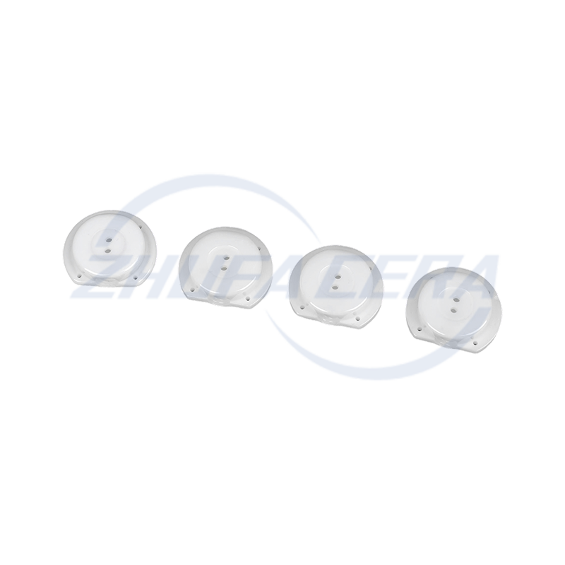
Zirconia ceramic wafers are representative products in the field of high-performance structural ceramics. Compared with traditional alumina ceramics or metal materials, its comprehensive performanc...
See Details -
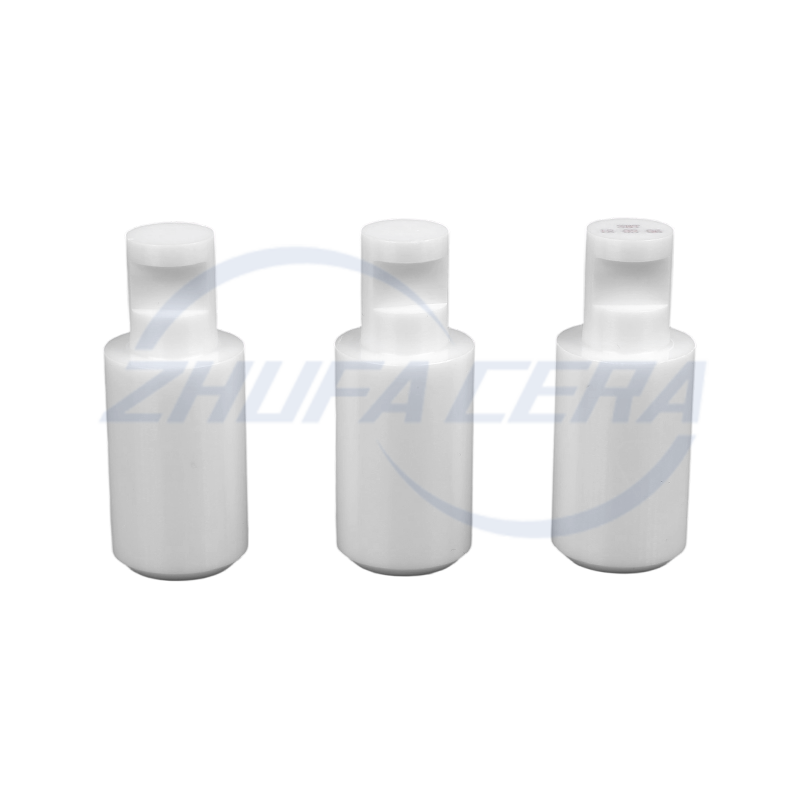
Zirconia Ceramic Plunger is a high-performance component designed for harsh industrial environments. Compared with similar ceramic or metal plunger products, it stands out with its unique material adv...
See Details


-
Quick Links
Home Products About Us Services Technology News Contact Us -
Products
Ceramic Structural Parts Zirconia Ceramics Alumina Ceramics ZTA Ceramics Silicon Nitride Ceramics Silicon Carbide Ceramics Ceramic Injection Molded Parts -
About Us
Factory Tour Honor FAQ -
Contact info
+86-188 8878 5188zf@zfcera.comNo. 1, Xinggong Road, Anchang Industrial Park, Keqiao District, Shaoxing City, Zhejiang Province, China -
WhatsApp

Copyright © Zhejiang Zhufa Precision Ceramics Technology Co., Ltd. All Rights Reserved.
China precision ceramics manufacturer
wholesale precision ceramics supplier
