

 中文简体
中文简体 русский
 Español
 عربى
عربى Português
 日本語
日本語 한국어
한국어
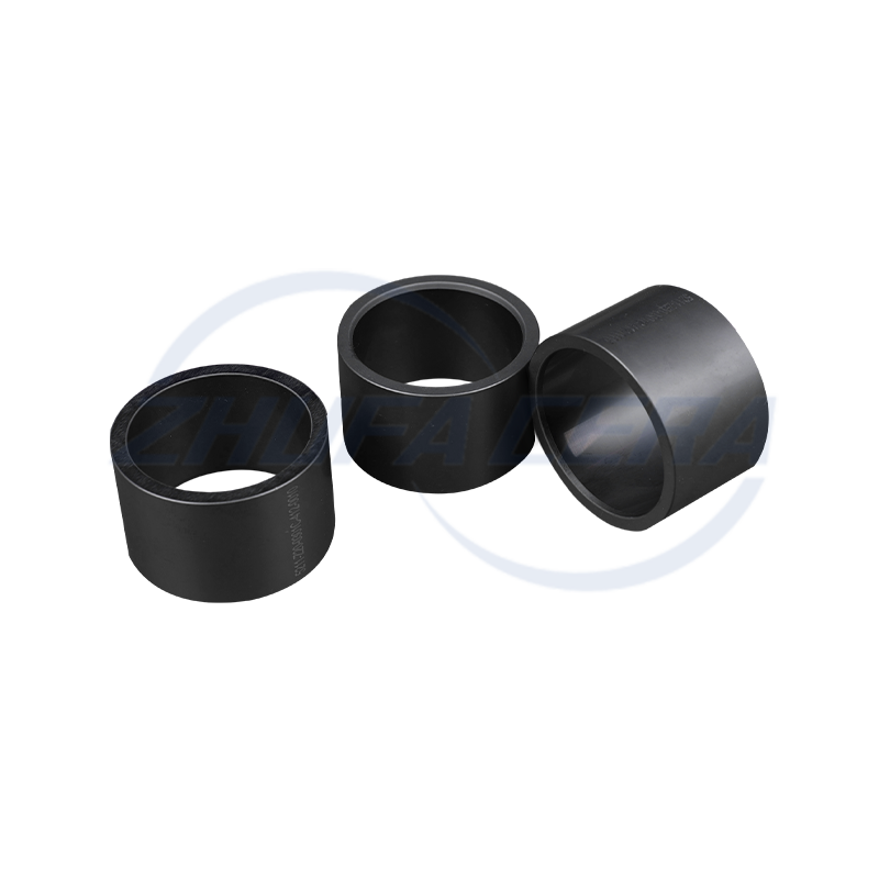
Black silicon carbide ceramic ring is a high-performance engineered ceramic assembly made of high-purity silicon carbide by precision molding and high temperature sintering. Its quadrangular crystal s...
See Details
FOLLOW US :


 Email: zf@zfcera.com
 Telephone: +86-188 8878 5188

How to design semiconductor component drawings that are easier to guide for precision ceramic processing?
2026-07-31
In semiconductor manufacturing equipment, precision ceramic components (such as electrostatic chucks (ESC), focus rings, insulating supports, vacuum chamber linings and other core positions) are widely used in core positions due to their superior high temperature resistance, plasma erosion resistance, high insulation and low thermal deformation characteristics. However, ceramic materials are inherently brittle materials with high hardness, no plastic deformation ability, and physical properties that are extremely sensitive to thermal stress and thermal shock. This means that traditional mechanical design thinking for metals or plastics completely fails in the field of ceramics - metals can absorb stress concentrations through localized plastic yielding, while ceramics only undergo brittle fracture when their elastic limit is exceeded. Therefore, to design precision ceramic drawings that truly take into account functional requirements and processing feasibility, design for manufacturability (DFM) must be integrated into the entire process of geometric configuration, tolerance system, assembly interface, and material properties.
1. Geometric configuration and processing technology limitations
From the perspective of geometric configuration optimization, the drawing design must comply with the process limits of modern ceramic processing technologies (such as diamond grinding, ultrasonic processing, laser cutting and green machining) to the greatest extent. In structural design, the elimination of stress concentration sources is the first principle. Sharp internal corners (such as right-angle transitions) should be avoided on drawings, because these areas can easily become the source of micro-crack initiation and expansion under the temperature stress field during the sintering process and subsequent mechanical processing, leading to processing edge chipping or service fracture. All internal corners must be designed as large as possible transition fillets (R corners); if right angles must be retained due to assembly requirements, undercut grooves or relief grooves must be added to the structure. At the same time, wall thickness uniformity is central to determining the quality of ceramic sintering. Since industrial ceramics are formed from powder and densified by high-temperature sintering, the huge difference in cross-sectional thickness will lead to uneven shrinkage, causing severe warping deformation, internal residual stress and even cracking. In addition, deep cavities, deep blind holes, and high aspect ratio structures should be strictly limited in feature design, because this will not only cause diamond grinding heads and ultrasonic machining tools to face severe insufficient stiffness and tool wear, but will also greatly worsen chip evacuation and cooling conditions.
2. Scientific trade-off between tolerance system and surface quality
When it comes to defining tolerance systems and surface quality, engineers must abandon the inertial thinking that “the higher the accuracy, the better.” Excessive tolerances are responsible for soaring machining costs and high scrap rates of technical ceramic components. Although advanced ceramics (such as aluminum oxide, aluminum nitride, silicon carbide) can achieve sub-micron dimensional accuracy through precision grinding, drawings must not impose strict tolerances on all dimensions without distinction. Dimensions that are not related to mating surfaces, free surfaces, or assembly positioning should be sufficiently relaxed to allow them to follow conventional green molding or sintering tolerances for ceramics. The labeling of surface roughness (Ra) must be targeted - the unprocessed sintered original surface usually has a higher roughness, while functional surfaces (such as wafer vacuum adsorption surface, dynamic seal precision alignment surface, high-frequency and high-voltage insulation surface) need to clearly specify the requirements for precision diamond grinding or polishing processing, and accurately weigh their actual impact on tribological performance, particle generation rate and vacuum sealing properties.
| Feature classification | Recommended tolerances / surface condition | Engineering Considerations and Design Points |
| Non-matching / free surface | General green/sintered tolerances (±0.1mm or percentage) | Fully relax size restrictions and reduce sintering scrap rate and processing costs. |
| Functional mating surface | Precision diamond grinding | Only the wafer adsorption, dynamic sealing or precise positioning are strictly controlled locally. |
| critical interface | Mirror polished grade (Ra < 0.05 μm) | Reduce the friction coefficient and strictly control the particle generation rate in the clean room. |
3. Assembly interface and thermal expansion adaptation
In addition, the extreme working conditions of semiconductor equipment determine that ceramic parts must be assembled with metal structural parts, which poses severe challenges to the assembly and fastening interface design in the drawings. Since hard ceramics cannot be directly tapped to create reliable threads (direct tapping can easily lead to tooth profile cracking or tooth slippage), the design of directly tapping internal threads on the ceramic body should be completely avoided in the drawings. Reasonable alternatives include: designing through holes with countersunk heads or steps, and using metal through-hole bolts for clamping and fixing; using high-temperature inorganic adhesives or hot sleeves with embedded metal inserts; or using precision pressure plates and flange structures to press ceramic parts onto the metal base. More critically, large differences in thermal expansion coefficients must be compensated for in drawings and fit tolerances. The thermal expansion coefficient of ceramics (such as alumina, silicon carbide) is much lower than that of structural metals such as stainless steel, aluminum alloys or titanium alloys. If sufficient thermal expansion gaps are not reserved between mating holes or pins during design, when the semiconductor cavity undergoes high-temperature processes (such as CVD, hot wall effect of Etch cavity, or high-temperature baking), since the expansion rate of metal is much greater than that of ceramics, extrusion stress will inevitably be generated on the ceramic parts, causing them to catastrophically fracture without warning.
4. Definition of key technical requirements
Finally, a mature and standardized semiconductor ceramic engineering drawing must have absolutely unambiguous definitions of material properties and post-processing processes in the technical requirements or title column. This mainly includes the following four core dimensions:
- Material grade and purity: For example, 6% or 99.9% high-purity alumina and reaction-sintered silicon carbide are used to strictly control the risk of contamination of advanced semiconductor processes by trace impurities such as alkali metals.
- Compactness and air tightness indicators: Clearly define whether the part needs to be absolutely dense with zero open pores (to meet the requirements of ultra-high vacuum environments), or whether a structure with a specific porosity is allowed.
- Edge Microprocessing Specifications: It is mandatory that all sharp edges be slightly chamfered or blunted (such as within 2 × 45° or R0.2) to eliminate microscopic burrs and prevent the generation of microscopic particles during clean room handling and assembly.
- Cleaning and packaging specifications: The final product is required to undergo ultrasonic cleaning and drying with high-purity deionized water, and be packaged in a vacuum double-layer package that meets semiconductor clean room standards.
Related products
-
-
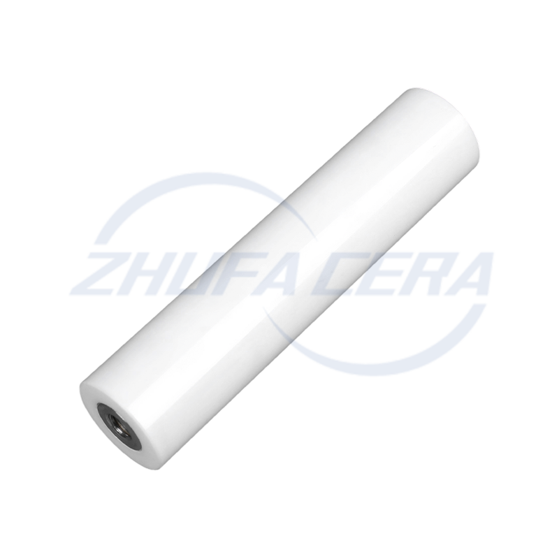
Zirconia Ceramic Rod is a high-performance ceramic material rod, mainly made of zirconium oxide, with excellent mechanical strength and chemical stability. It exhibits extremely high hardness and wear...
See Details -
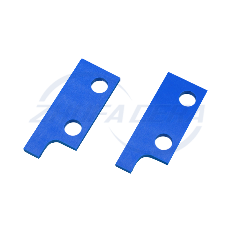
Blue zirconia ceramic sheets are precision components made of advanced zirconia ceramics. They are stained with cobalt, iron or copper to form a blue color. This color not only serves as a visual i...
See Details -

This blue zirconia ceramic pin is made of advanced zirconia ceramic material, providing excellent durability and performance. Zirconia ceramics are known for their high strength, good wear resistan...
See Details -

Zirconia Ceramic Gear is made of zirconium oxide ceramic material, which has excellent high strength and high hardness. This material property enables it to effectively resist wear during the transmis...
See Details -
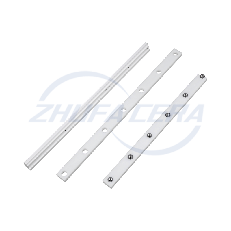
Zirconia Ceramic Guide Rail is a high-performance precision mechanical component made of zirconium oxide ceramic material. Its core characteristics are derived from the excellent physical and chemical...
See Details -
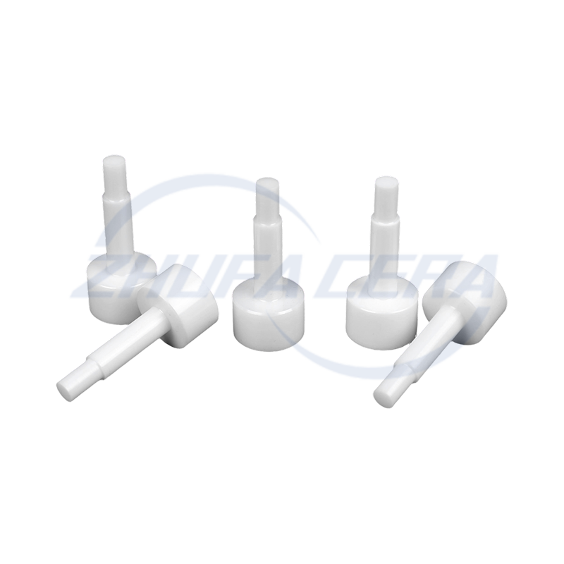
Zirconia Ceramic Locating Pin is a high-precision positioning element made of advanced zirconium oxide ceramic material with excellent physical and chemical properties. Its main characteristics includ...
See Details -
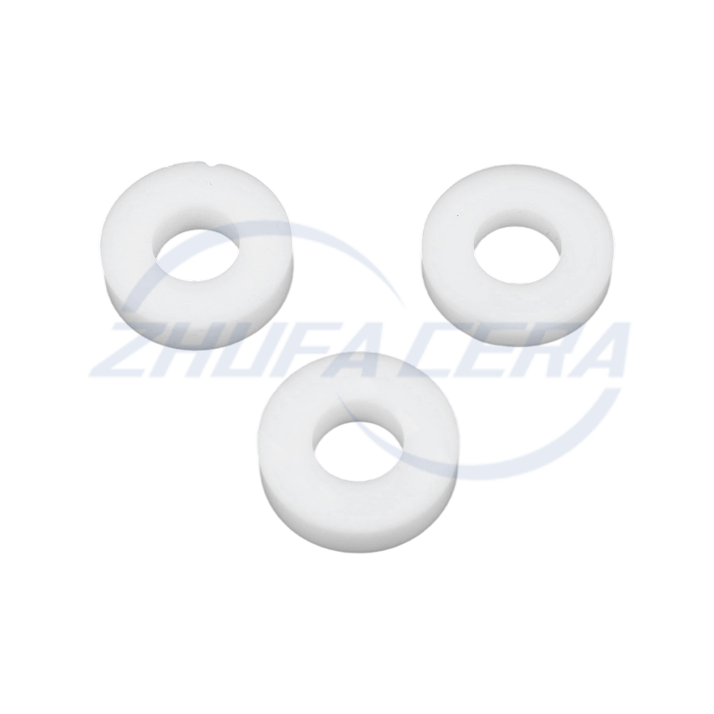
Zirconia Ceramic Ring is a high-performance ceramic product known for its excellent physical and chemical properties. It has extremely high hardness and strength, with a Mohs hardness of more than 8.5...
See Details -
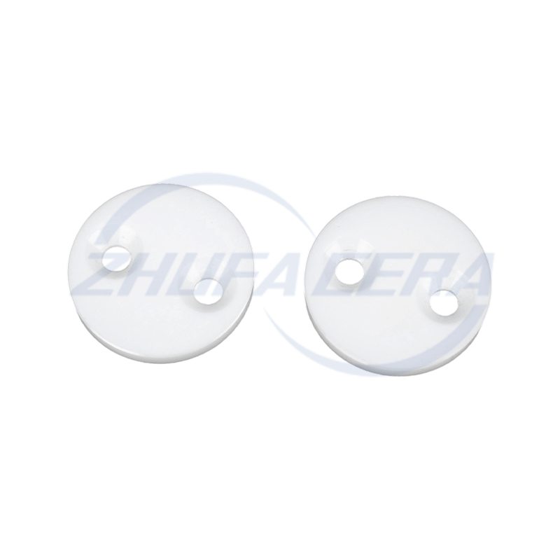
Zirconia ceramic sheets have become functional core components in various fields thanks to their unique properties. With a flexural strength of 900–1200 MPa and a fracture toughness of 6–10 MPa・m¹/², ...
See Details -

Zirconia Ceramic Strip is a strip material made of high-performance zirconium oxide ceramic with excellent physical and chemical properties. It has extremely high hardness and flexural strength, can e...
See Details -
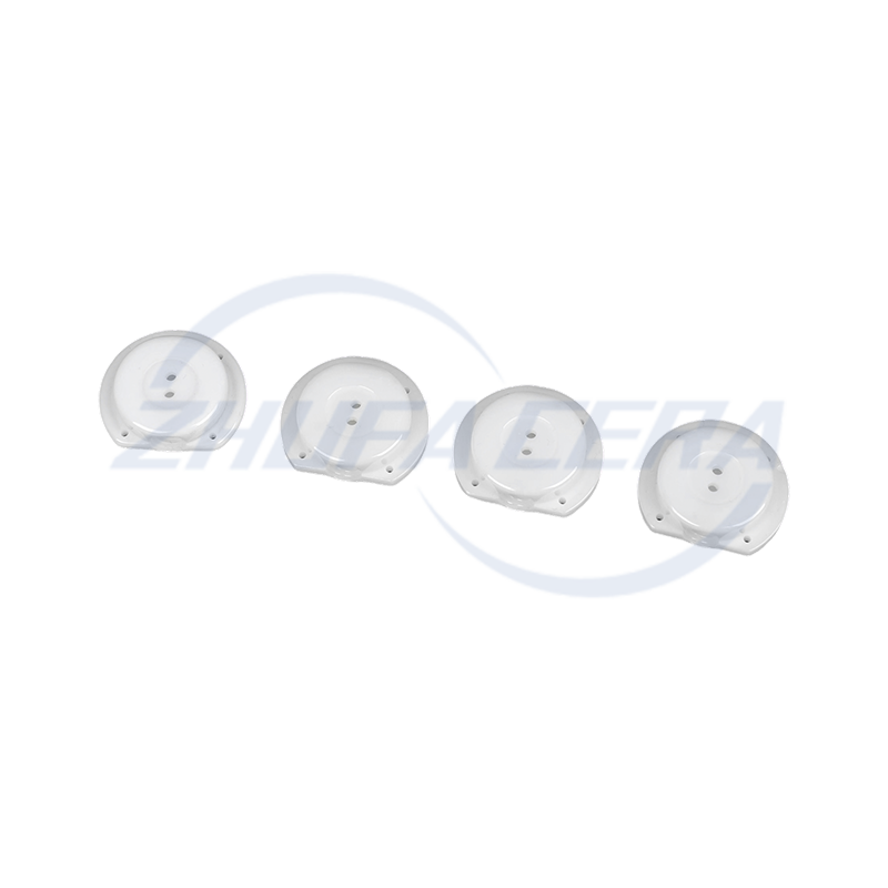
Zirconia ceramic wafers are representative products in the field of high-performance structural ceramics. Compared with traditional alumina ceramics or metal materials, its comprehensive performanc...
See Details -
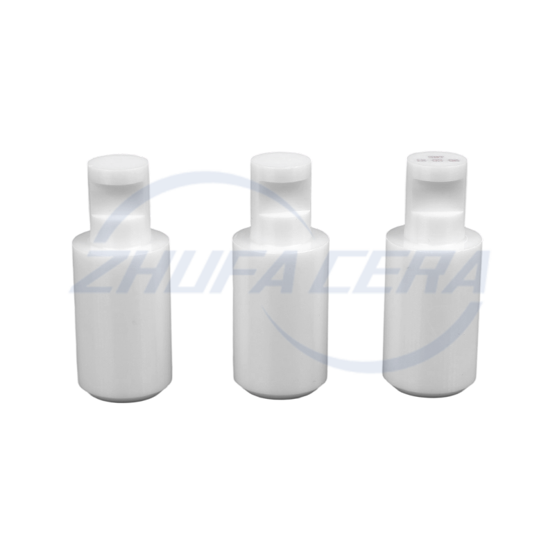
Zirconia Ceramic Plunger is a high-performance component designed for harsh industrial environments. Compared with similar ceramic or metal plunger products, it stands out with its unique material adv...
See Details


-
Quick Links
Home Products About Us Services Technology News Contact Us -
Products
Ceramic Structural Parts Zirconia Ceramics Alumina Ceramics ZTA Ceramics Silicon Nitride Ceramics Silicon Carbide Ceramics Ceramic Injection Molded Parts -
About Us
Factory Tour Honor FAQ -
Contact info
+86-188 8878 5188zf@zfcera.comNo. 1, Xinggong Road, Anchang Industrial Park, Keqiao District, Shaoxing City, Zhejiang Province, China -
WhatsApp

Copyright © Zhejiang Zhufa Precision Ceramics Technology Co., Ltd. All Rights Reserved.
China precision ceramics manufacturer
wholesale precision ceramics supplier
