

 中文简体
中文简体 русский
 Español
 عربى
عربى Português
 日本語
日本語 한국어
한국어
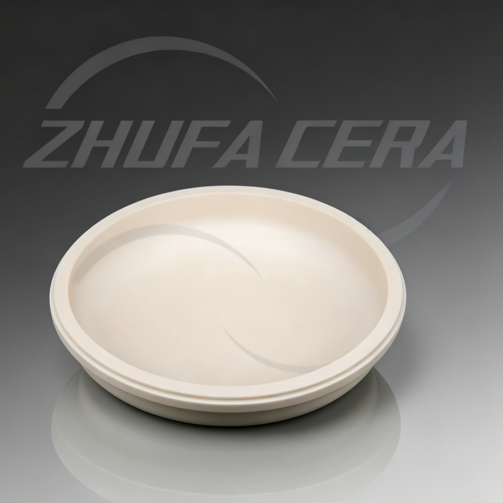
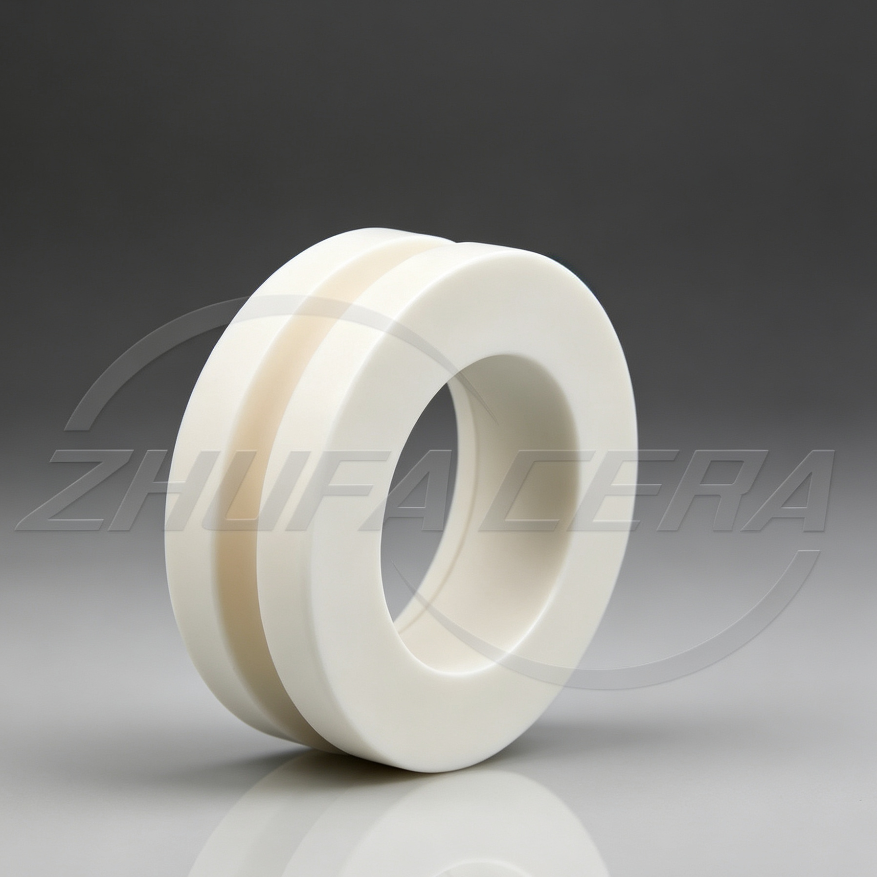
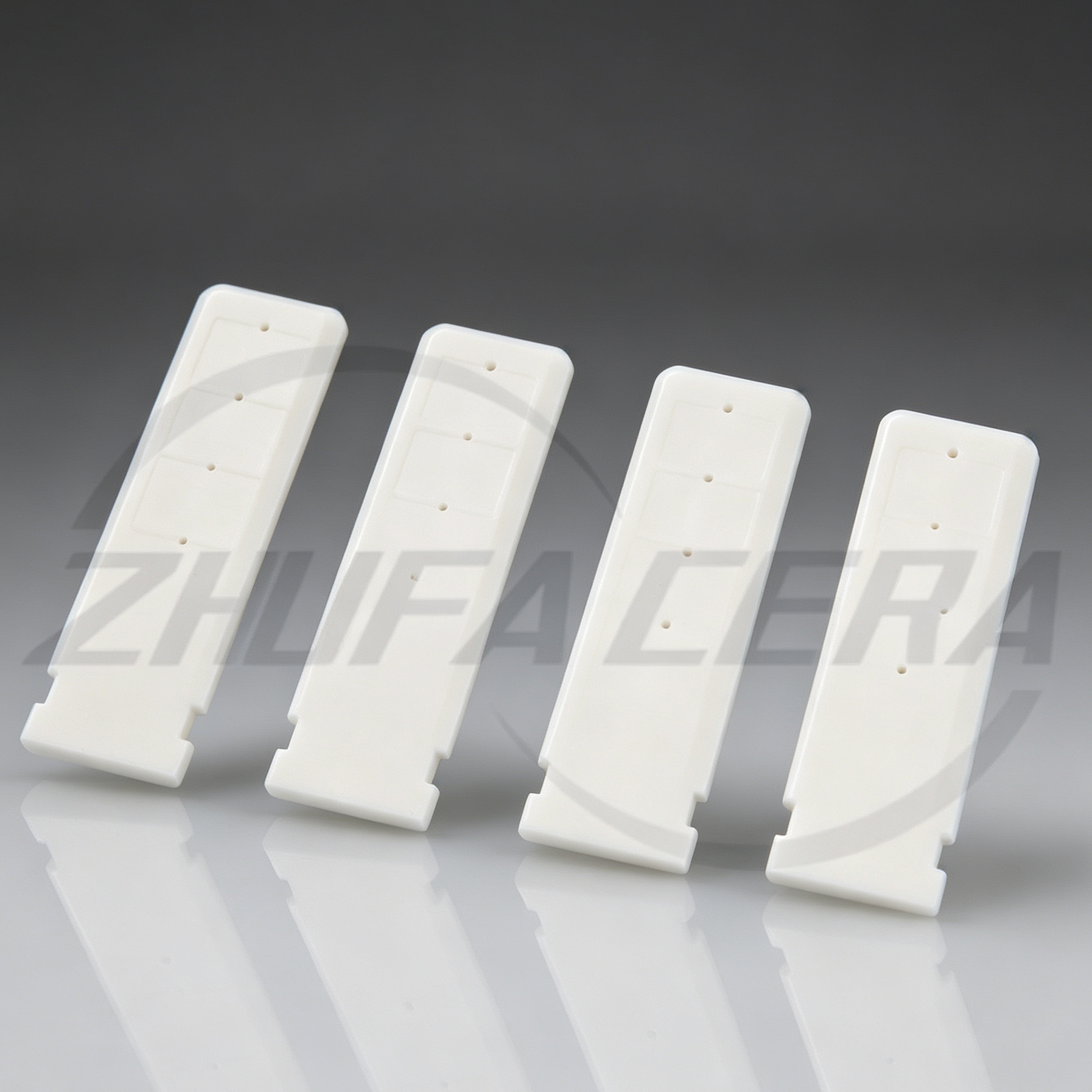
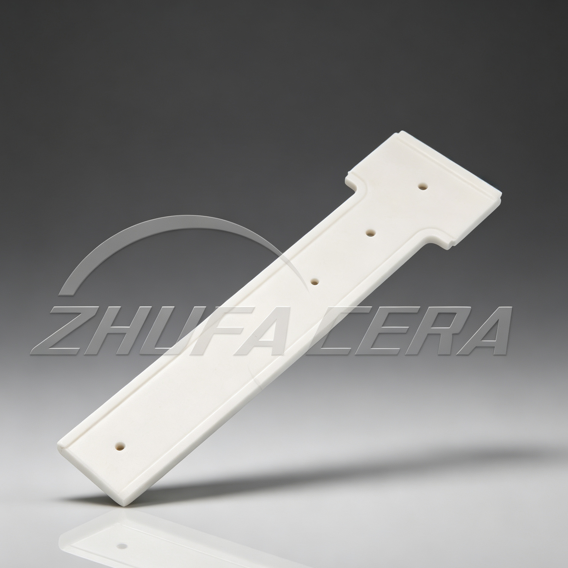
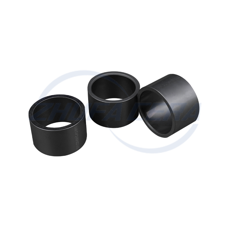
Black silicon carbide ceramic ring is a high-performance engineered ceramic assembly made of high-purity silicon carbide by precision molding and high temperature sintering. Its quadrangular crystal s...
See Details
FOLLOW US :


 Email: zf@zfcera.com
 Telephone: +86-188 8878 5188

How to improve the surface roughness of the wafer carrier through the ceramic mirror grinding process?
2026-07-25
In the semiconductor manufacturing and precision processing supply chain, the wafer carrier is the core supporting component, and its surface quality directly determines the wafer's bonding accuracy, vacuum adsorption flatness, and overall process yield. For purchasing decision-makers and engineers at home and abroad who are responsible for semiconductor equipment, photolithography or etching modules, looking for the ability to stably deliver nanometer-level surface finish (such as Ra ≤ 0.02 μm ) suppliers are the key to ensuring high-end performance of equipment.
Whether it is high-purity alumina, silicon carbide or silicon nitride, advanced ceramics have “ Hard, brittle and difficult to process ” typical characteristics. Traditional mechanical grinding can easily lead to surface micro-cracks, edge chipping and sub-surface damage, which often become a source of particle pollution in clean rooms. To meet semiconductor customers' stringent surface integrity standards, top ceramic manufacturers are rolling out “ Ductile domain (plastic) grinding ” and related advanced technologies.
1. Realizing ductile domain grinding and composite auxiliary technology
In order to achieve mirror-level effects while ensuring structural strength, the processing end mainly uses the following two breakthrough technologies, which are also important indicators for procurement to evaluate the technological maturity of suppliers:
- Craft one ELID Online electrolytic sharpening grinding: Use a metal-bonded (such as cast iron or bronze base) diamond grinding wheel, and use a special electrolytic device to perform real-time, micro-electrolytic sharpening of the grinding wheel during the grinding process. The electrolysis continuously dissolves the surface metal bond, allowing the fine diamond abrasive grains to remain sharp and exposed, avoiding crushing and breakage caused by passivation of the grinding wheel.
- Craft two Ultrasonic vibration-assisted grinding: Introduce high-frequency, micro-amplitude mechanical vibration to the grinding wheel or workpiece system, causing the abrasive particles to cause periodic vibrations on the ceramic surface. “ impact - Micro cutting ” status. This significantly reduces cutting force and instantaneous frictional heat, and completely suppresses macroscopic spalling and edge chipping of grains.
2. Rigorous screening and dressing of grinding wheels and abrasives
The precision of the grinding tool directly maps and determines the final micromorphology of the workpiece:
- Micro abrasives and precision dressing: In the fine grinding stage, a diamond grinding wheel with finer grain size (such as W5 至 W10 even finer grained), and the grinding wheel circular runout is controlled within 1 μm within, avoid Tiny beats leave spiral machining marks on the ceramic surface.
- Multi-pass composite polishing connection: Mirror grinding usually requires micron / Nano-scale diamond abrasive paste is used for step-by-step transition polishing to completely eliminate microscopic cracks and meet the integration requirements of pollution-free clean rooms.
Three. Ultimate control of grinding motion parameters and machine tool systems
- Micron depth of cut and low feed rates: Strictly control the depth of a single cut to the sub-micron level ( 0.5 ~ 2 μm/pass ), forcing the material to undergo microscopic plastic rheology rather than disintegration, and at the same time, combined with low feed speeds, avoids micro-vibration marks caused by instantaneous cutting force fluctuations.
- Ultra-high rigidity machine tools and environmentally friendly cooling: Ultra-precision surface grinders using high-damping materials (such as granite or high-strength cast iron bed), combined with high-flow, high-pressure precision coolant, can wash away fine grinding debris in a timely manner to prevent secondary scratches, ensuring that every carrier plate delivered to the purchaser has near-perfect cleanliness and smoothness.
Four. Typical product sharing
In advanced process semiconductor equipment, in addition to the wafer carrier, many core functional components also rely heavily on mirror grinding technology to break through the limits of physical performance. The following is an in-depth analysis of the engineering characteristics, material selection and key indicators of mirror processing of four types of high-tech barrier ceramic structural parts:
| 1. Semiconductor electrostatic chuck ( ESC ) Ceramic dielectric layer and carrier substrate Mainstream materials: 99.9% High purity alumina or sintered silicon carbide. Key technical indicators: surface roughness Ra ≤ 0.015 μm , flatness ≤ 3 μm (full format), parallelism < 5 μm 。 Technical value and necessity of mirror grinding: The electrostatic chuck needs to use Coulomb force or Johnson force when working. - Rabe ック( J-R ) effect strongly adsorbs silicon wafers. If there are microscopic roughness or microcracks on the load-bearing surface, it is easy to cause local air gap micro-discharge under a high voltage of several thousand volts, thus breaking down the dielectric layer and damaging the wafer. Pass ELID The composite process of ultra-precision mirror grinding and chemical machine polishing can completely eliminate sub-surface damage and ensure the uniformity of heat conduction on the back and the reliability of high-voltage insulation. | [Core structure diagram] Ra ≤ 0.02 μm |
| 2. Reaction Chamber Plasma Etching Focusing Ring Mainstream materials: High-purity single-phase sintered silicon carbide or high-density quartz replacement silicon nitride 。 Key technical indicators: Joint surface flatness ≤ 5 μm , side wall and step surface finish Ra ≤ 0.05 μm 。 Technical value and necessity of mirror grinding: The focus ring surrounds the silicon wafer and is directly exposed to strong fluorine / bombarded by chlorine-based plasma. Excessive microscopic roughness will increase the rate of plasma chemical erosion and produce exfoliated particles that contaminate the wafer. Precision grinding can optimize the grain boundary bonding state, reduce microscopic stress concentration, and significantly extend its service life in the etching cavity. | [Core structure diagram] Ra ≤ 0.02 μm |
| 3. Ceramic reference ruler for photolithography machines Mainstream materials: Zero Thermal Expansion Crystallized Glass Ceramic 或 High rigidity hot pressed silicon carbide. Key technical indicators: linear expansion coefficient < 1.0×10⁻⁶/K , surface roughness Ra ≤ 0.01 μm , the local flatness reaches sub-micron level. Technical value and necessity of mirror grinding: As the core benchmark for optical alignment and positioning, these components have zero tolerance for thermal deformation and geometric errors. Ultrasonic-assisted grinding and nano-level grinding ensure the sharpness and long-term geometric stability of the engraved line reference, which directly determines the overlay accuracy of the lithography machine. | [Core structure diagram] Ra ≤ 0.02 μm |
| 4. Semiconductor ultra-precision air-bearing guide rails and sliders Mainstream materials: High-density alumina ceramics ( Al₂O₃ ) or reaction sintered silicon carbide. Key technical indicators: Guide surface straightness ≤ 1 μm / 300mm , surface roughness Ra ≤ 0.02 μm , hardness HRA > 88 。 Technical value and necessity of mirror grinding: The micron-scale air film is used between the air bearing guide rail and the air bearing to achieve frictionless suspension motion. If there are micron-level knife marks or ripples on the working surface of the guide rail, it will directly cause air film turbulence, vibration and “ crawl ” phenomenon. The extremely high surface density and extremely low friction coefficient brought by mirror grinding are the prerequisites for realizing high-speed and smooth movement of nano-scale CNC positioning platforms. | [Core structure diagram] Ra ≤ 0.02 μm |
5. How to choose a reliable supplier of precision ceramics?
| For purchasing decision makers, when evaluating semiconductor structural ceramic suppliers, in addition to reviewing basic processing quotations, they should also focus on penetrating the following three core supply chain indicators: 1. Process closed loop and core equipment: Verify whether the supplier has ELID Online electrolytic sharpening grinders, ultrasonic auxiliary machining centers and a complete set of nano-scale grinding and polishing production lines can avoid tolerance accumulation and quality control caused by multiple outsourcing processes. 2. Detection and traceability capabilities: Suppliers are required to provide white light interferometers, high-precision three-dimensional coordinate measuring instruments and helium mass spectrometry leak detection reports to ensure that components such as carrier plates and electrostatic chucks delivered in each batch comply with Ra ≤ 0.02 μm And there are no strict standards for micro cracks. 3. Engineering customization and failure analysis support: Evaluate whether its technical team can assist in material grade matching and structural optimization design based on the working environment provided by the customer (such as specific plasma concentration, high-voltage insulation requirements). If you are looking for a reliable partner that can provide customized, high-precision semiconductor structural ceramics and core components such as wafer carriers and electrostatic chucks, please feel free to contact us for detailed material data sheets and customized solutions. |
Related products
-
-
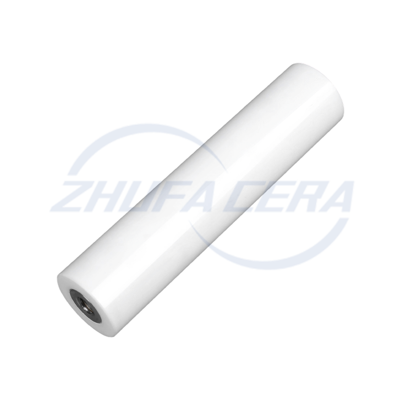
Zirconia Ceramic Rod is a high-performance ceramic material rod, mainly made of zirconium oxide, with excellent mechanical strength and chemical stability. It exhibits extremely high hardness and wear...
See Details -
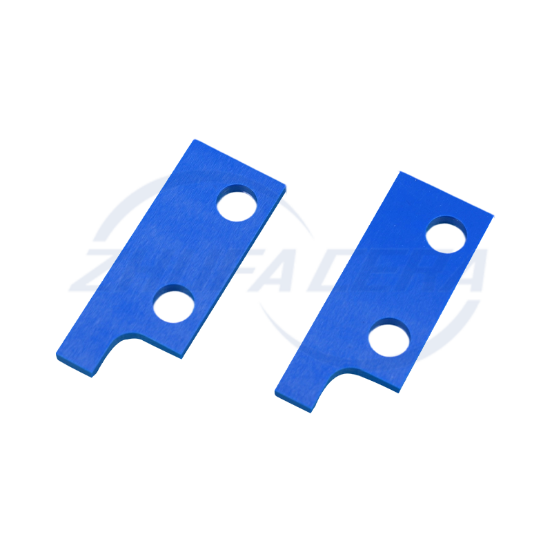
Blue zirconia ceramic sheets are precision components made of advanced zirconia ceramics. They are stained with cobalt, iron or copper to form a blue color. This color not only serves as a visual i...
See Details -
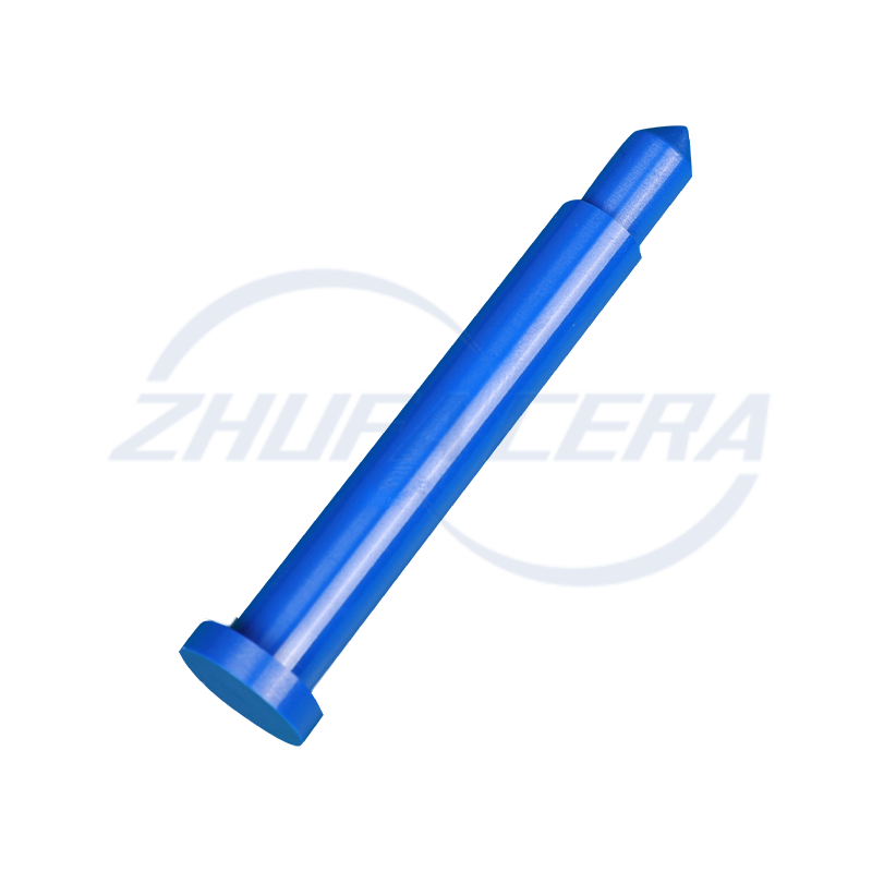
This blue zirconia ceramic pin is made of advanced zirconia ceramic material, providing excellent durability and performance. Zirconia ceramics are known for their high strength, good wear resistan...
See Details -

Zirconia Ceramic Gear is made of zirconium oxide ceramic material, which has excellent high strength and high hardness. This material property enables it to effectively resist wear during the transmis...
See Details -
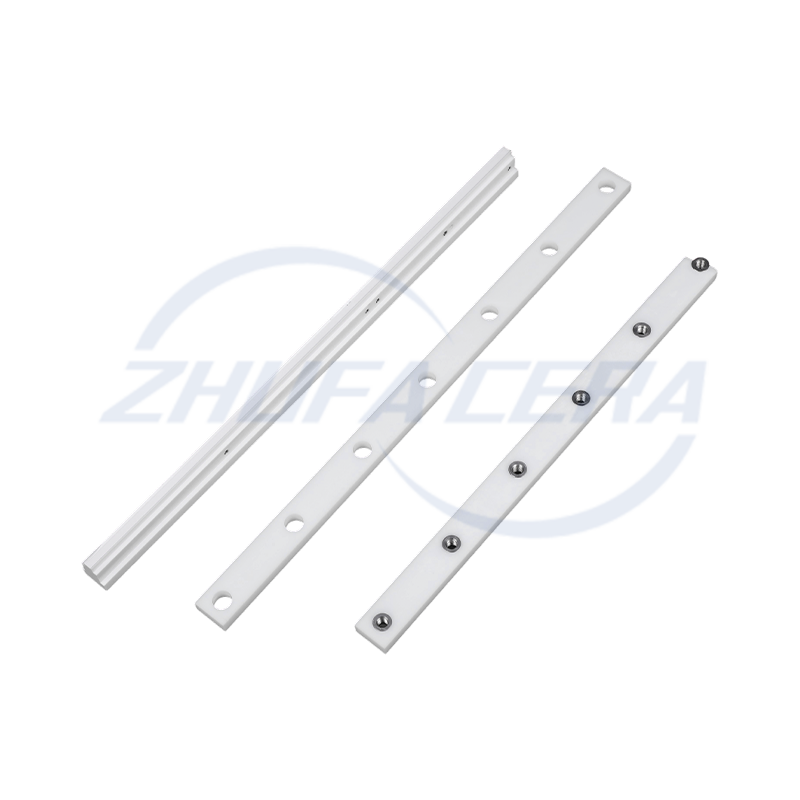
Zirconia Ceramic Guide Rail is a high-performance precision mechanical component made of zirconium oxide ceramic material. Its core characteristics are derived from the excellent physical and chemical...
See Details -
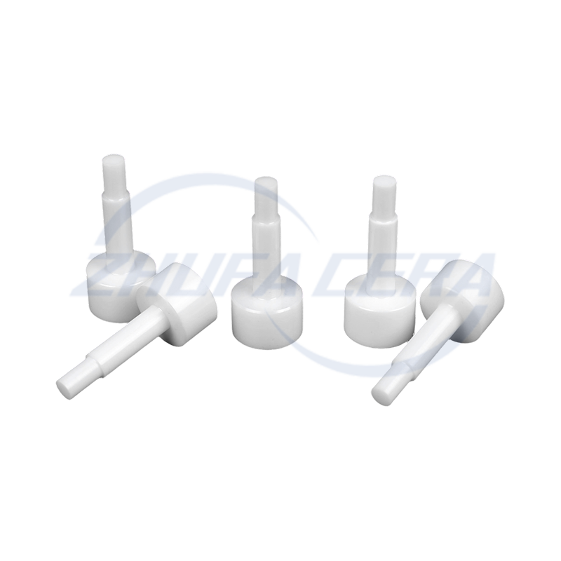
Zirconia Ceramic Locating Pin is a high-precision positioning element made of advanced zirconium oxide ceramic material with excellent physical and chemical properties. Its main characteristics includ...
See Details -
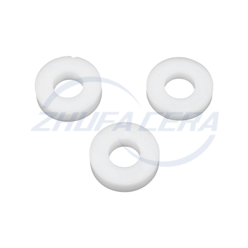
Zirconia Ceramic Ring is a high-performance ceramic product known for its excellent physical and chemical properties. It has extremely high hardness and strength, with a Mohs hardness of more than 8.5...
See Details -
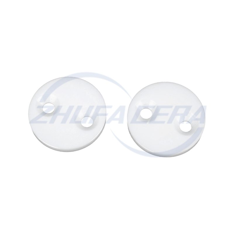
Zirconia ceramic sheets have become functional core components in various fields thanks to their unique properties. With a flexural strength of 900–1200 MPa and a fracture toughness of 6–10 MPa・m¹/², ...
See Details -
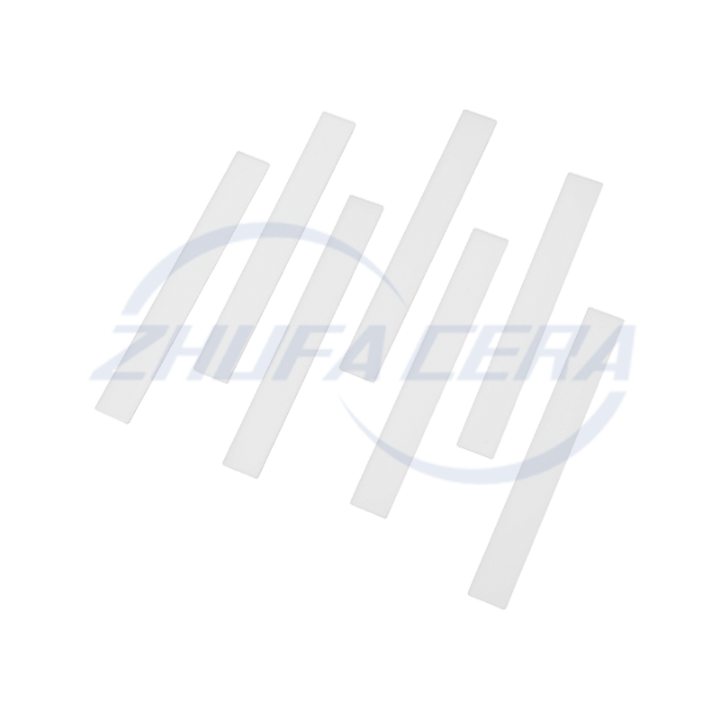
Zirconia Ceramic Strip is a strip material made of high-performance zirconium oxide ceramic with excellent physical and chemical properties. It has extremely high hardness and flexural strength, can e...
See Details -
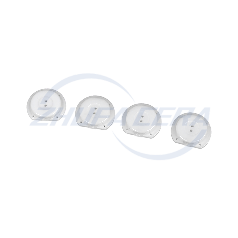
Zirconia ceramic wafers are representative products in the field of high-performance structural ceramics. Compared with traditional alumina ceramics or metal materials, its comprehensive performanc...
See Details -
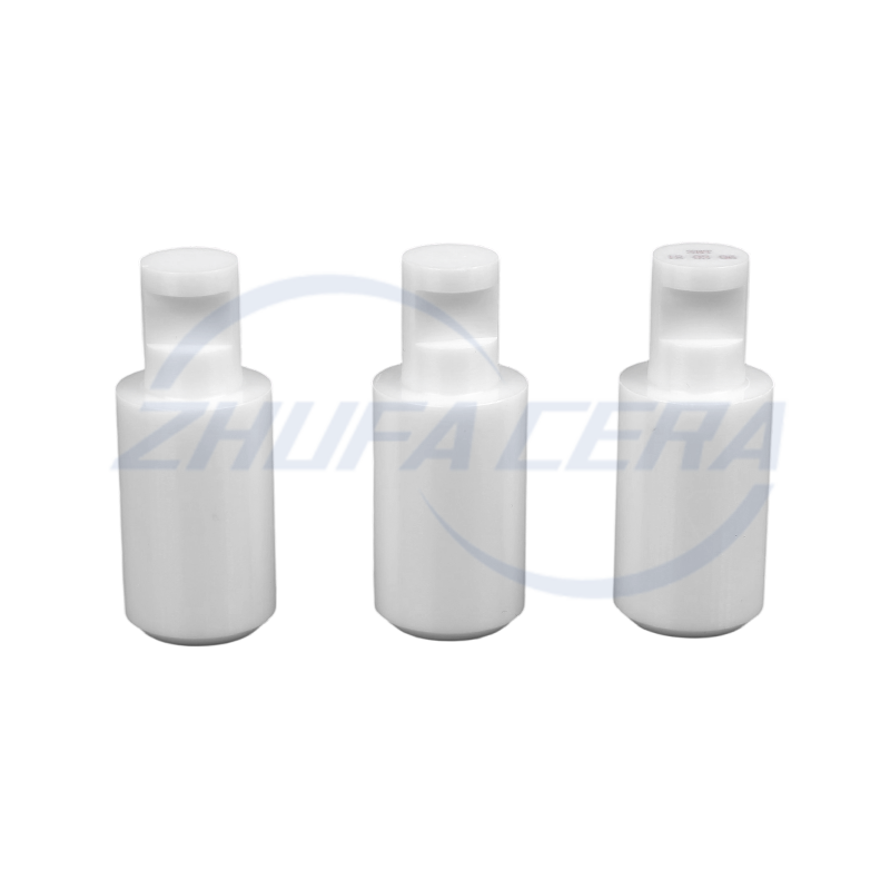
Zirconia Ceramic Plunger is a high-performance component designed for harsh industrial environments. Compared with similar ceramic or metal plunger products, it stands out with its unique material adv...
See Details


-
Quick Links
Home Products About Us Services Technology News Contact Us -
Products
Ceramic Structural Parts Zirconia Ceramics Alumina Ceramics ZTA Ceramics Silicon Nitride Ceramics Silicon Carbide Ceramics Ceramic Injection Molded Parts -
About Us
Factory Tour Honor FAQ -
Contact info
+86-188 8878 5188zf@zfcera.comNo. 1, Xinggong Road, Anchang Industrial Park, Keqiao District, Shaoxing City, Zhejiang Province, China -
WhatsApp

Copyright © Zhejiang Zhufa Precision Ceramics Technology Co., Ltd. All Rights Reserved.
China precision ceramics manufacturer
wholesale precision ceramics supplier
