

 中文简体
中文简体 русский
 Español
 عربى
عربى Português
 日本語
日本語 한국어
한국어
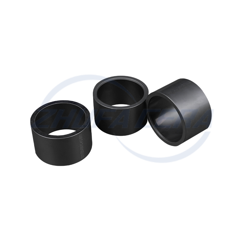
Black silicon carbide ceramic ring is a high-performance engineered ceramic assembly made of high-purity silicon carbide by precision molding and high temperature sintering. Its quadrangular crystal s...
See Details
FOLLOW US :


 Email: zf@zfcera.com
 Telephone: +86-188 8878 5188

Why is micron-level precision ceramic processing indispensable?
2026-07-20
| core feed Today, as semiconductor manufacturing is moving toward Sub-7nm and even more advanced processes, photolithography machines, as the "crown jewel" of chip manufacturing, have improved their overlay accuracy to the nanometer level (nm). Under the extreme conditions of ultra-high-speed step scanning motion with acceleration exceeding 10g, extremely high heat flux density, and ultra-high vacuum of 10⁻⁷ Pa, traditional metal materials such as titanium alloy and Invar alloy have reached their physical limits. Advanced structural ceramics (silicon carbide, aluminum nitride, aluminum oxide) have become irreplaceable ultimate structural materials in photolithography machines and core semiconductor equipment due to their high specific stiffness, extremely low thermal expansion coefficient, high thermal conductivity and excellent vacuum compatibility. |
01 Extreme working conditions: The physical bottleneck of traditional metals in photolithography equipment
The wafer exposure process of the photolithography machine requires the system to complete high-speed positioning and stabilization within milliseconds. When faced with this extreme engineering challenge, traditional metal components have exposed three fatal shortcomings:
- Insufficient dynamic stiffness causes mechanical resonance: During frequent starts and stops and high-speed acceleration, the elastic modulus/density ratio (specific stiffness) of metal materials is limited, which is prone to minor structural deformations and high-frequency aftershocks, greatly prolonging alignment time and degrading optical focus accuracy.
- Thermal expansion causes focus drift: The high-energy laser beam and plasma radiation inside the lithography machine will cause local temperature rise. The thermal expansion coefficient of metal materials is high, and micron-level thermal deformation will cause the depth of focus to lose focus, causing the entire wafer to be scrapped.
- Ultra-high vacuum degassing and particulate contamination: Metal materials are prone to release trace amounts of gas in ultra-high vacuum environments, and are prone to peeling off particles when bombarded by highly corrosive plasma, contaminating expensive optical lenses and reaction chambers.
02 Material Dimensionality Reduction Strike: Performance Comparison of Advanced Structural Ceramics
In order to overcome the above physical bottlenecks, advanced structural ceramics have become the inevitable choice for lithography machine engineers. The following table compares the core physical properties of semiconductor-grade advanced ceramics and commonly used high-precision metal materials:
| Material name | Density ρ (g/cm³) | Modulus of elasticity E (GPa) | Specific stiffness E/ρ (GPa·cm³/g) | Coefficient of thermal expansion CTE (×10⁻⁶/K) | Thermal conductivity k (W/m·K) |
| Titanium alloy | 4.43 | 114 | 25.7 | 8.6 | 6.7 |
| Invar | 8.05 | 141 | 17.5 | 1.2 | 10.1 |
| High purity alumina | 3.92 | 380 | 96.9 | 7.2 | 30.0 |
| aluminum nitride | 3.26 | 310 | 95.1 | 4.5 | 170-220 |
| silicon carbide | 3.10 | 410-450 | 132-145 | 4.0 | 120-200 |
[Performance summary]: The specific stiffness of silicon carbide is more than 5 times that of titanium alloy, the thermal conductivity is close to that of aluminum alloy, and the thermal expansion coefficient is only a fraction of that of metal. It is the material of choice for high-speed and ultra-precision moving components.
03 Core application: Decomposition of key ceramic components of photolithography machine
- Wafer Dual Workpiece Stage
[Leading material]: reaction sintering/pressureless sintered silicon carbide
[Application Analysis]: The workpiece stage carries the wafer to complete millisecond-level high-speed scanning. The ultra-lightweight SiC frame using a topologically optimized hollow structure can reduce weight by more than 40% while maintaining extremely high bending stiffness, allowing the workpiece table to achieve "zero deformation" under extremely high acceleration of 10g, ensuring nanometer-level overlay accuracy.
- Electrostatic chuck base
[Main material]: Aluminum nitride/aluminum oxide
[Application Analysis]: The electrostatic chuck uses Coulomb force to adsorb the wafer flatly. AlN has extremely high thermal conductivity and excellent electrical insulation. Micron-level molybdenum/tungsten heating wires are embedded inside through a co-firing process, and tens of thousands of microneedle arrays are processed on the surface. While achieving uniform and rapid temperature control, it greatly reduces the contact area with the wafer and avoids particle contamination.
- Laser interferometer reference mirror/mirror strip
[Leading Materials]: Zero-expansion glass-ceramic/reaction-sintered silicon carbide
[Application Analysis]: It is used as a laser reference reflective surface for interferometric measurement of the position of the dual workpiece stage in the X/Y/Z axis direction. Its surface roughness is required to reach Ra < 0.1 nm, and it is required to maintain absolute dimensional stability under temperature control fluctuations to ensure nanosecond-level response and nanometer-level accuracy of the ranging optical path.
- Wafer transfer gripper
[Leading material]: High-purity alumina/silicon nitride
[Application Analysis]: Used to connect 300mm (12-inch) wafers between reaction chambers at extremely high speed. The mechanical gripper requires extremely high cantilever stiffness and wear resistance to ensure that it does not bend, sag, or drop chips when swinging at high speed.
04 Manufacturing barriers: core technical difficulties in micron-level precision ceramic processing
| Description of engineering difficulties "Sintering is just to get the entry ticket, micron-level finishing is the decisive point." Ceramic materials have high hardness (Mohs hardness 8.5~9.5) and high brittleness. To process the sintered blank into the final component that meets the requirements of semiconductors, four major engineering problems need to be overcome. |
- Ultra-precision geometric tolerance control: For the 12-inch electrostatic chuck and SiC workpiece table, the global flatness within the full size range is required to be controlled within ≤ 1 µm (equivalent to 1/70 of the diameter of a hair), and the position tolerance of micropores and complex flow channels is locked at ±2 µm.
- Nanoscale ultra-smooth polishing and surface damage suppression: Grinding can easily leave microscopic cracks on the surface of hard and brittle ceramics, which can cause instantaneous brittle fracture under strong stress. Chemical mechanical polishing (CMP) and ultra-precision grinding technology must be used to eliminate micro-cracks while improving the roughness of the wafer contact surface to a mirror level of Ra < 0.1 nm.
- Manufacturing of complex inner cavities and lightweight topologies: In order to meet the needs of weight reduction and cooling, SiC components are often designed with honeycomb hollow structures and embedded microfluidics. This requires extremely high-precision five-axis diamond CNC engraving and milling capabilities and advanced non-destructive testing (NDT) methods.
- Ultra-high vacuum cleanliness treatment: The processed ceramic parts need to undergo multiple ultrasonic degreasing, strong acid/strong alkali cleaning, and high-temperature baking and air blasting to completely eliminate processing residues in micropores and blind holes, ensuring that the outgassing rate approaches zero under 10⁻⁷ Pa vacuum after installation.
05 Conclusion and Outlook
Competition in the semiconductor industry, on the surface, is a battle between chip design and photolithography processes, but at its base it is a hard-core duel between material science and ultra-precision processing technology. Micron-level precision ceramic processing technology not only represents the pinnacle of advanced manufacturing technology, but also is the core key to supporting the next generation of high-capacity, ultra-high-precision lithography machines and high-end semiconductor equipment to become independent and controllable.
Related products
-
-
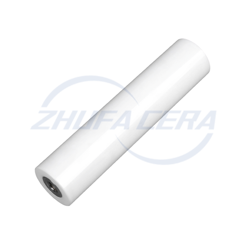
Zirconia Ceramic Rod is a high-performance ceramic material rod, mainly made of zirconium oxide, with excellent mechanical strength and chemical stability. It exhibits extremely high hardness and wear...
See Details -
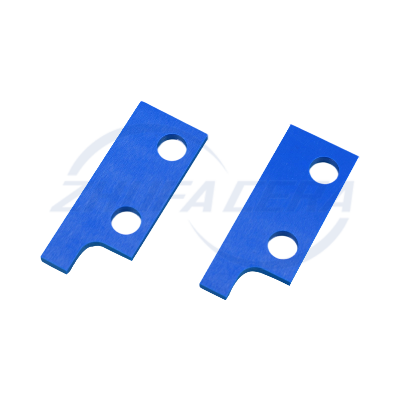
Blue zirconia ceramic sheets are precision components made of advanced zirconia ceramics. They are stained with cobalt, iron or copper to form a blue color. This color not only serves as a visual i...
See Details -

This blue zirconia ceramic pin is made of advanced zirconia ceramic material, providing excellent durability and performance. Zirconia ceramics are known for their high strength, good wear resistan...
See Details -

Zirconia Ceramic Gear is made of zirconium oxide ceramic material, which has excellent high strength and high hardness. This material property enables it to effectively resist wear during the transmis...
See Details -
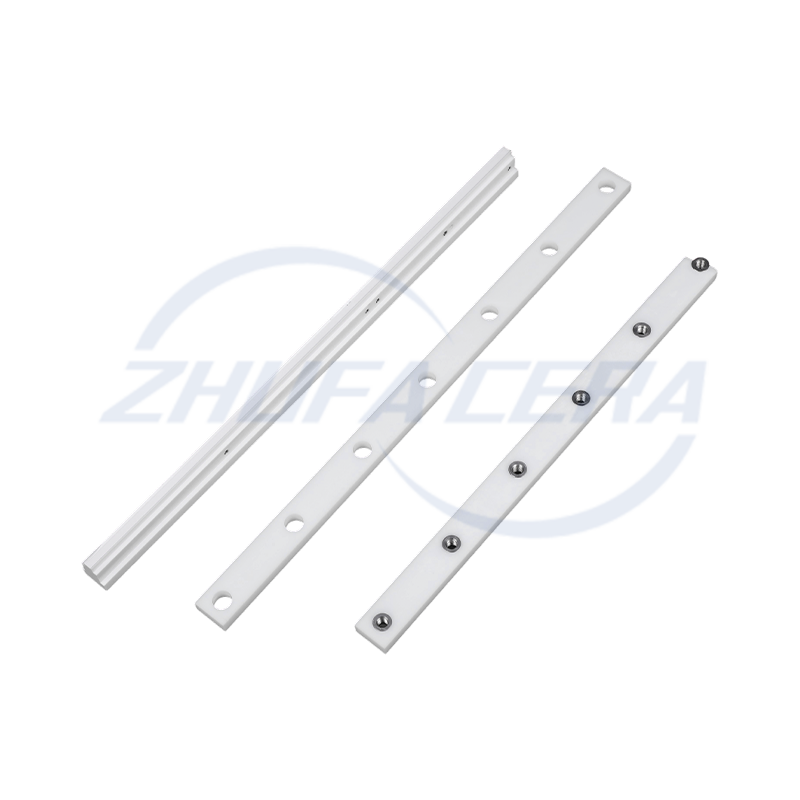
Zirconia Ceramic Guide Rail is a high-performance precision mechanical component made of zirconium oxide ceramic material. Its core characteristics are derived from the excellent physical and chemical...
See Details -
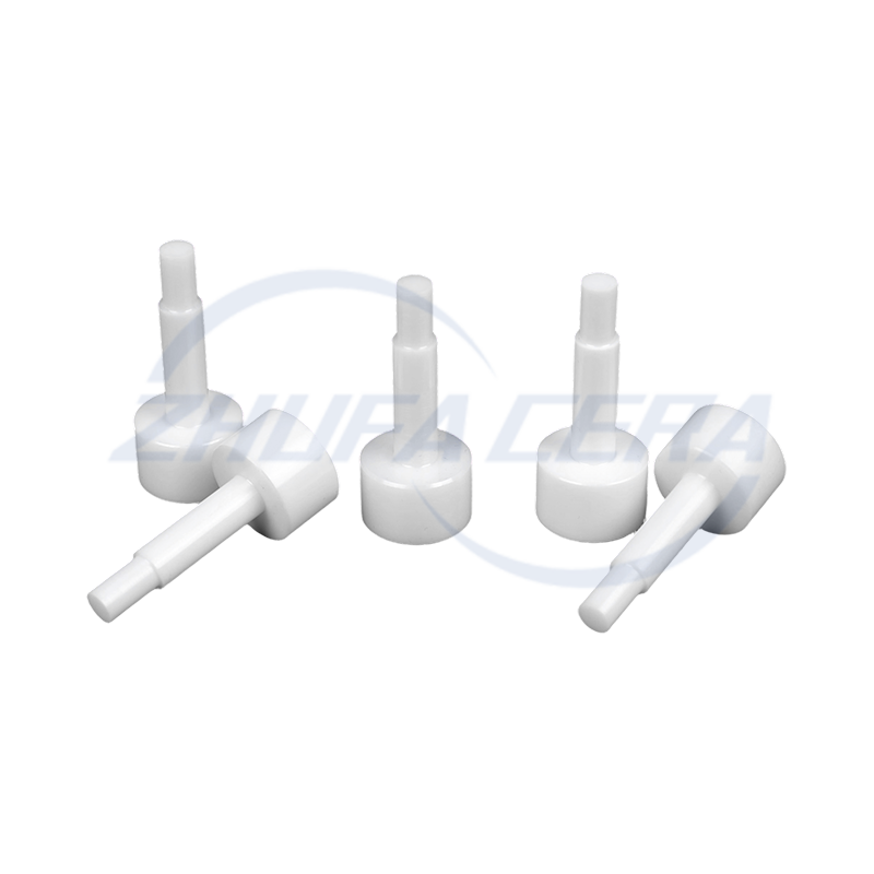
Zirconia Ceramic Locating Pin is a high-precision positioning element made of advanced zirconium oxide ceramic material with excellent physical and chemical properties. Its main characteristics includ...
See Details -
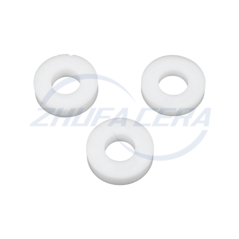
Zirconia Ceramic Ring is a high-performance ceramic product known for its excellent physical and chemical properties. It has extremely high hardness and strength, with a Mohs hardness of more than 8.5...
See Details -
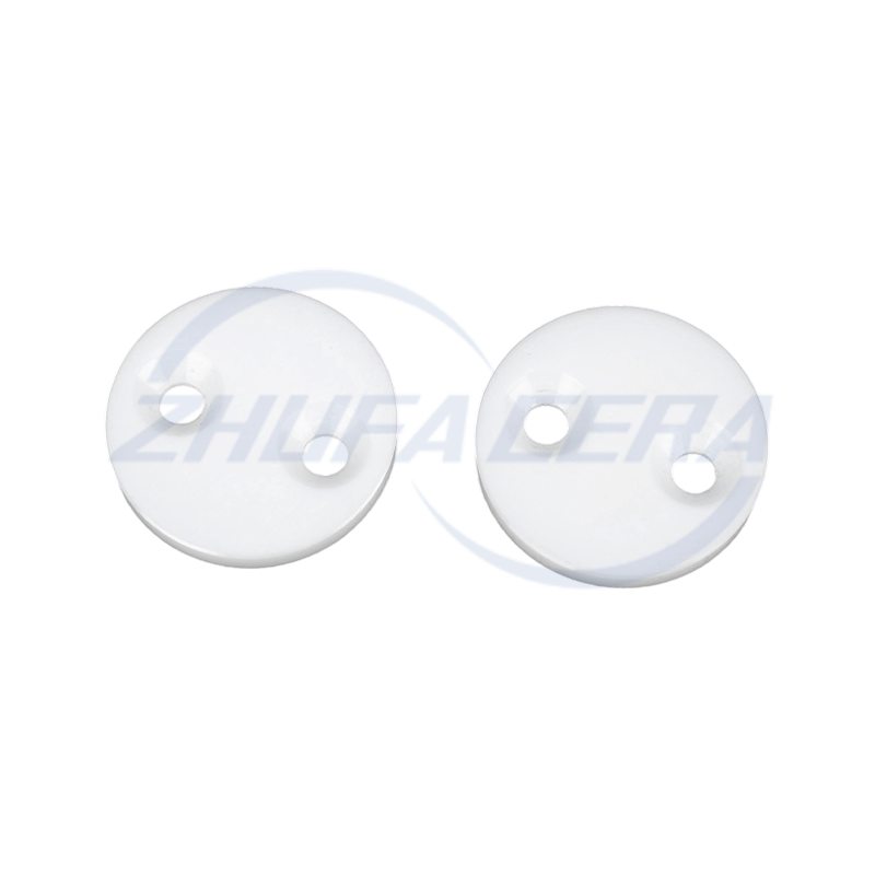
Zirconia ceramic sheets have become functional core components in various fields thanks to their unique properties. With a flexural strength of 900–1200 MPa and a fracture toughness of 6–10 MPa・m¹/², ...
See Details -

Zirconia Ceramic Strip is a strip material made of high-performance zirconium oxide ceramic with excellent physical and chemical properties. It has extremely high hardness and flexural strength, can e...
See Details -
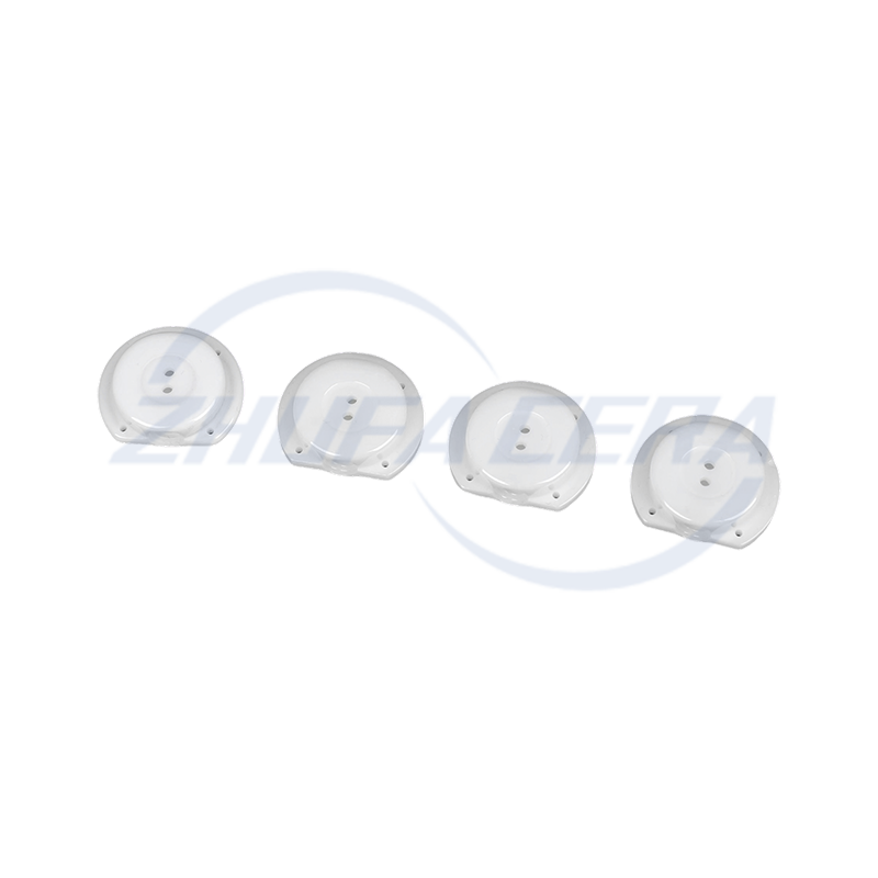
Zirconia ceramic wafers are representative products in the field of high-performance structural ceramics. Compared with traditional alumina ceramics or metal materials, its comprehensive performanc...
See Details -
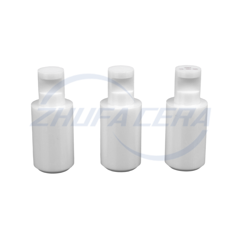
Zirconia Ceramic Plunger is a high-performance component designed for harsh industrial environments. Compared with similar ceramic or metal plunger products, it stands out with its unique material adv...
See Details


-
Quick Links
Home Products About Us Services Technology News Contact Us -
Products
Ceramic Structural Parts Zirconia Ceramics Alumina Ceramics ZTA Ceramics Silicon Nitride Ceramics Silicon Carbide Ceramics Ceramic Injection Molded Parts -
About Us
Factory Tour Honor FAQ -
Contact info
+86-188 8878 5188zf@zfcera.comNo. 1, Xinggong Road, Anchang Industrial Park, Keqiao District, Shaoxing City, Zhejiang Province, China -
WhatsApp

Copyright © Zhejiang Zhufa Precision Ceramics Technology Co., Ltd. All Rights Reserved.
China precision ceramics manufacturer
wholesale precision ceramics supplier
