中文简体
中文简体 русский
 Español
 عربى
عربى Português
 日本語
日本語 한국어
한국어

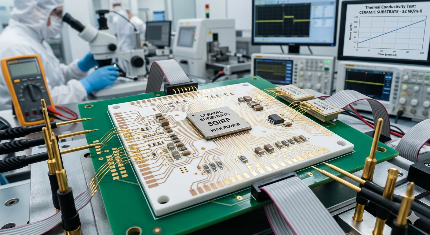
A ceramic substrate is a thin, rigid plate made from advanced ceramic materials — such as alumina, aluminum nitride, or beryllium oxide — used as the foundational layer in electronic packaging, power modules, and circuit assemblies. It matters because it combines exceptional thermal conductivity, electrical insulation, and mechanical stability in ways that traditional polymer or metal substrates simply cannot match, making it indispensable across the EV, 5G, aerospace, and medical industries.
What Is a Ceramic Substrate? A Clear Definition
A ceramic substrate serves as both a mechanical support and a thermal/electrical interface in high-performance electronic systems. Unlike printed circuit boards (PCBs) made from epoxy-glass composites, ceramic substrates are sintered from inorganic, non-metallic compounds, giving them superior performance at extreme temperatures and under high-power conditions.
The term "substrate" in electronics refers to the base material onto which other components — transistors, capacitors, resistors, metal traces — are deposited or bonded. In ceramic substrates, this base layer itself becomes a critical engineering component rather than a passive carrier.
The global ceramic substrate market was valued at approximately USD 8.7 billion in 2023 and is projected to reach over USD 16.4 billion by 2032, driven by the explosive growth of electric vehicles, 5G base stations, and power semiconductors.
Key Types of Ceramic Substrates: Which Material Fits Your Application?
The most commonly used ceramic substrate materials each offer distinct trade-offs between cost, thermal performance, and mechanical properties. Choosing the right type is critical to system reliability and longevity.
1. Alumina (Al₂O₃) Ceramic Substrate
Alumina is the most widely used ceramic substrate material, accounting for over 60% of global production volume. With a thermal conductivity of 20–35 W/m·K, it balances performance and affordability. Purity levels range from 96% to 99.6%, with higher purity delivering better dielectric properties. It is widely used in consumer electronics, automotive sensors, and LED modules.
2. Aluminum Nitride (AlN) Ceramic Substrate
AlN ceramic substrates offer the highest thermal conductivity among mainstream options, reaching 170–230 W/m·K — nearly 10× that of alumina. This makes them ideal for high-power laser diodes, IGBT modules in electric vehicles, and RF power amplifiers in 5G infrastructure. The trade-off is significantly higher manufacturing cost compared to alumina.
3. Silicon Nitride (Si₃N₄) Ceramic Substrate
Silicon nitride substrates excel in mechanical toughness and fracture resistance, making them the preferred choice for automotive power modules subjected to thermal cycling. With a thermal conductivity of 70–90 W/m·K and a flexural strength exceeding 700 MPa, Si₃N₄ outperforms AlN in vibration-heavy environments such as EV drivetrains and industrial inverters.
4. Beryllium Oxide (BeO) Ceramic Substrate
BeO substrates provide exceptional thermal conductivity of 250–300 W/m·K, the highest of any oxide ceramic. However, beryllium oxide powder is toxic, making manufacturing hazardous and its use strictly regulated. BeO is primarily found in military radar systems, aerospace avionics, and high-power traveling-wave tube amplifiers.
Ceramic Substrate Material Comparison
| Material | Thermal Conductivity (W/m·K) | Flexural Strength (MPa) | Relative Cost | Primary Applications |
| Alumina (Al₂O₃) | 20–35 | 300–400 | Low | Consumer electronics, LEDs, sensors |
| Aluminum Nitride (AlN) | 170–230 | 300–350 | High | EV power modules, 5G, laser diodes |
| Silicon Nitride (Si₃N₄) | 70–90 | 700–900 | Medium-High | Automotive inverters, traction drives |
| Beryllium Oxide (BeO) | 250–300 | 200–250 | Very High | Military radar, aerospace, TWTAs |
Caption: Comparison of the four primary ceramic substrate materials by thermal performance, mechanical strength, cost, and typical end-use application.
How Are Ceramic Substrates Manufactured?
Ceramic substrates are produced through a multi-step sintering process that transforms raw powder into dense, precisely dimensioned plates. Understanding the manufacturing flow helps engineers specify tolerances and surface finishes correctly.
Step 1 – Powder Preparation and Mixing
High-purity ceramic powder is blended with organic binders, plasticizers, and solvents to create a slurry. Purity control at this stage directly influences the dielectric constant and thermal conductivity of the finished substrate.
Step 2 – Tape Casting or Dry Pressing
The slurry is either cast into thin sheets (tape casting, for multilayer substrates) or uniaxially pressed into green compacts. Tape casting produces layers as thin as 0.1 mm, enabling LTCC (Low Temperature Co-fired Ceramic) multilayer structures used in RF modules.
Step 3 – Debinding and Sintering
The green body is heated to 1,600–1,800°C in controlled atmospheres (nitrogen for AlN to prevent oxidation) to burn off organic binders and densify the ceramic grains. This step determines final porosity, density, and dimensional accuracy.
Step 4 – Metallization
Conductive traces are applied using one of three main techniques: DBC (Direct Bonded Copper), AMB (Active Metal Brazing), or thick-film printing with silver/platinum pastes. DBC dominates in power electronics because it bonds copper directly to ceramic at the eutectic temperature (~1,065°C), creating a robust metallurgical joint without adhesives.
Ceramic Substrate vs. Other Substrate Types: A Direct Comparison
Ceramic substrates outperform FR4 PCBs and metal-core PCBs at high power densities, though they carry higher unit cost. The right substrate depends on operating temperature, power dissipation, and reliability requirements.
| Property | Ceramic Substrate | FR4 PCB | Metal-Core PCB (MCPCB) |
| Thermal Conductivity (W/m·K) | 20–230 | 0.3–0.5 | 1–3 |
| Max Operating Temp (°C) | 350–900+ | 130–150 | 140–160 |
| Dielectric Constant (at 1 MHz) | 8–10 (Al₂O₃) | 4.0–4.7 | ~4.5 |
| CTE (ppm/°C) | 4–7 | 14–17 | 16–20 |
| Relative Material Cost | High | Low | Medium |
| Hermetic Sealing | Yes | No | No |
Caption: Head-to-head comparison of ceramic substrates against FR4 PCBs and metal-core PCBs across key thermal, electrical, and cost parameters.
Where Are Ceramic Substrates Used? Key Industry Applications
Ceramic substrates are deployed wherever power density, reliability, and temperature extremes eliminate polymer alternatives. From the battery management system in an EV to the transceiver inside a satellite, ceramic substrates appear across a remarkable breadth of industries.
- Electric Vehicles (EVs): AlN and Si₃N₄ substrates in IGBT/SiC power modules manage inverter switching losses and withstand 150,000+ thermal cycles over the vehicle lifetime. A typical EV traction inverter contains 6–12 ceramic substrate-based power modules.
- 5G Telecommunications: LTCC multilayer ceramic substrates enable miniaturized RF front-end modules (FEMs) that operate at millimeter-wave frequencies (24–100 GHz) with low signal loss and stable dielectric properties.
- Industrial Power Electronics: High-power motor drives and solar inverters rely on DBC ceramic substrates to dissipate hundreds of watts per module continuously.
- Aerospace and Defense: BeO and AlN substrates withstand -55°C to +200°C cycling in avionics, missile guidance electronics, and phased-array radar systems.
- Medical Devices: Biocompatible alumina substrates are used in implantable defibrillators and hearing aids where hermeticity and long-term stability are non-negotiable.
- High-Power LEDs: Alumina ceramic substrates replace FR4 in high-luminance LED arrays for stadium lighting and horticultural grow lights, enabling junction temperatures below 85°C at 5W+ per LED.
DBC vs. AMB Ceramic Substrates: Understanding the Metallization Difference
DBC (Direct Bonded Copper) and AMB (Active Metal Brazing) represent two fundamentally different approaches to bonding copper to ceramic, each with distinct strengths for specific power density and thermal cycling requirements.
In DBC, copper foil is bonded to alumina or AlN at ~1,065°C via a copper-oxygen eutectic. This produces a very thin bond interface (essentially zero adhesive layer), yielding excellent thermal performance. DBC on AlN can carry current densities above 200 A/cm².
AMB uses active braze alloys (typically silver-copper-titanium) to bond copper to Si₃N₄ at 800–900°C. The titanium reacts chemically with the ceramic surface, enabling the bonding of copper to nitride ceramics that cannot be DBC-processed. AMB substrates on Si₃N₄ demonstrate superior power cycling reliability — over 300,000 cycles at ΔT = 100 K — making them the industry standard for automotive traction inverters.
Emerging Trends in Ceramic Substrate Technology
Three emerging trends are reshaping ceramic substrate design: the shift to wide-bandgap semiconductors, 3D embedded packaging, and sustainability-driven manufacturing.
Wide-Bandgap Semiconductors (SiC and GaN)
SiC MOSFETs and GaN HEMTs switch at frequencies of 100 kHz–1 MHz, generating heat fluxes above 500 W/cm². This pushes thermal management requirements beyond what traditional alumina substrates can handle, driving rapid adoption of AlN and Si₃N₄ ceramic substrates in next-generation power modules.
3D Heterogeneous Integration
LTCC multilayer ceramic substrates now enable 3D integration of passive components (capacitors, inductors, filters) directly within substrate layers, reducing component count by up to 40% and shrinking module footprint — critical for next-generation phased-array antennas and automotive radar.
Green Manufacturing Processes
Pressure-assisted sintering techniques such as spark plasma sintering (SPS) reduce densification temperatures by 200–300°C and processing time from hours to minutes, cutting energy consumption in AlN substrate production by an estimated 35%.
Frequently Asked Questions About Ceramic Substrates
Q1: What is the difference between a ceramic substrate and a ceramic PCB?
A ceramic PCB is a finished circuit board built on a ceramic substrate. The ceramic substrate itself is the bare base material — the rigid ceramic plate — while a ceramic PCB includes metallized traces, vias, and surface finishes ready for component mounting. All ceramic PCBs use ceramic substrates, but not all ceramic substrates become PCBs (some are used purely as heat spreaders or mechanical supports).
Q2: Can ceramic substrates be used with lead-free soldering processes?
Yes. Ceramic substrates with nickel/gold (ENIG) or nickel/silver surface finishes are fully compatible with SAC (tin-silver-copper) lead-free solder alloys. The thermal mass and CTE of the ceramic must be factored into reflow profiling to prevent cracking during rapid thermal ramp-up. A typical safe ramp rate is 2–3°C per second for alumina substrates.
Q3: Why do ceramic substrates have better CTE matching to silicon than FR4?
Silicon has a CTE of ~2.6 ppm/°C. Alumina's CTE is ~6–7 ppm/°C, and AlN is ~4.5 ppm/°C — both significantly closer to silicon than FR4's 14–17 ppm/°C. This mismatch reduction minimizes solder joint and die-attach fatigue during thermal cycling, directly extending the operational lifetime of power semiconductor packages from thousands to hundreds of thousands of cycles.
Q4: How thick are typical ceramic substrates?
Standard thicknesses range from 0.25 mm to 1.0 mm for most power electronics applications. Thinner substrates (0.25–0.38 mm) reduce thermal resistance but are more fragile. High-power DBC substrates are typically 0.63 mm to 1.0 mm thick. LTCC multilayer substrates for RF applications may range from 0.1 mm per tape layer up to several millimeters total stack height.
Q5: What surface finish options are available for ceramic substrates?
Common metallization surface finishes include: bare copper (for immediate die-attach or soldering), Ni/Au (ENIG — most common for wire bonding compatibility), Ni/Ag (for lead-free soldering), and silver or platinum-based thick films for resistor networks. The choice depends on bonding method (wire bonding, flip-chip, soldering) and hermeticity requirements.
Conclusion: Is a Ceramic Substrate Right for Your Application?
A ceramic substrate is the right choice whenever thermal performance, long-term reliability, and operating temperature exceed the capabilities of polymer alternatives. If your application involves power densities above 50 W/cm², operating temperatures exceeding 150°C, or more than 10,000 thermal cycles over its lifetime, a ceramic substrate — whether alumina, AlN, or Si₃N₄ — will deliver reliability that FR4 or MCPCBs structurally cannot.
The key is material selection: use alumina for cost-sensitive, moderate-power applications; AlN for maximum thermal dissipation; Si₃N₄ for vibration and power cycling durability; and BeO only where regulations permit and no alternative exists. With the power electronics market accelerating through EV adoption and 5G rollout, ceramic substrates will only grow more central to modern electronics engineering.
Engineers specifying substrates should request material datasheets for thermal conductivity, CTE, and flexural strength, and validate metallization options against their soldering and bonding processes. Prototype testing across the expected thermal cycle range remains the single most reliable predictor of field performance.