
 中文简体
中文简体 русский
 Español
 عربى
عربى Português
 日本語
日本語 한국어
한국어
Black silicon carbide ceramic ring is a high-performance engineered ceramic assembly made of high-purity silicon carbide by precision molding and high temperature sintering. Its quadrangular crystal s...
See Details
FOLLOW US :


 Email: zf@zfcera.com
 Telephone: +86-188 8878 5188

Why Semiconductor Ceramic Components Require High-Cost Post-Machining Cleaning
2026-06-12
Even when semiconductor precision ceramic components (such as Aluminum Oxide (Al₂O₃), Silicon Nitride (Si₃N₄), and Silicon Carbide (SiC)) achieve a mirror-like finish after precision machining, they cannot be directly deployed into core wafer fabrication equipment (e.g., Etchers, CVD systems).
Instead, they must undergo an incredibly complex and costly ultra-clean purification process. This requirement is driven not only by the semiconductor industry's "zero-tolerance" policy for wafer contamination but also by the unique microstructural characteristics—namely, the brittle nature and inherent porosity—of advanced ceramics. This article provides a deep dive into the core causes and technical barriers behind the high cost of semiconductor ceramic cleaning.
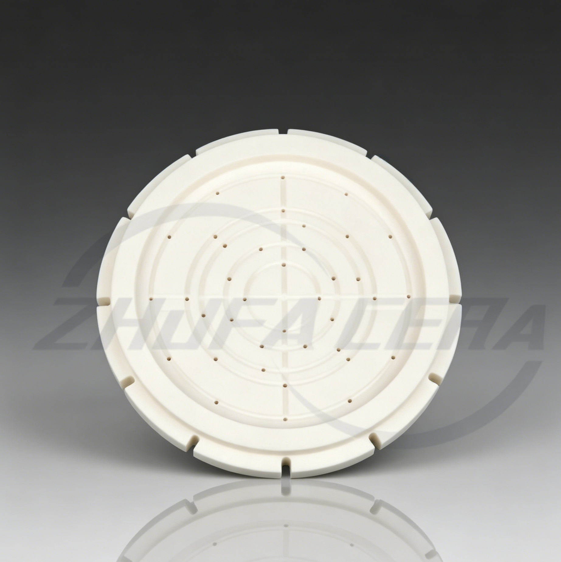
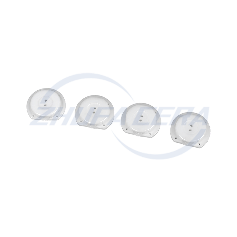
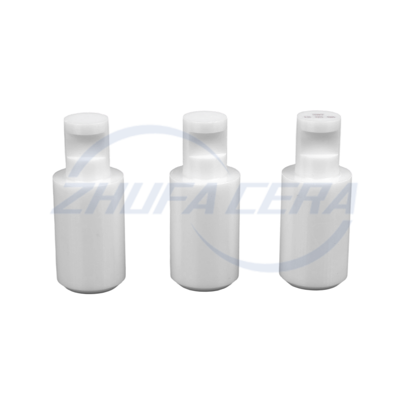
Representative Semiconductor Ceramic Components
- The Threat of "Microscopic Residues"
In advanced node wafer fabrication (e.g., 3nm, 5nm), even sub-nanometer physical or chemical contamination can lead to catastrophic yield loss. Standard machining processes—such as turning, milling, grinding, and polishing—leave behind three primary types of critical contaminants on the ceramic surface:
- Transition Metal Ions (The Most Fatal): Wear from carbide cutting tools and contact with fixtures introduce metal ions such as Copper (Cu), Iron (Fe), Chromium (Cr), and Nickel (Ni). If these ions volatilize inside the vacuum chamber and diffuse into the silicon substrate, they degrade the electrical performance of the semiconductor devices, causing severe leakage currents or dielectric breakdown.
- Chemical & Organic Medium Residues: Machining fluids, polishing pastes, rust-preventative oils, and coolants leave behind complex macromolecular organics. When exposed to the high-vacuum, high-intensity plasma environment of a process chamber, these organics undergo rapid outgassing. This destabilizes chamber vacuum levels and cross-contaminates the entire wafer processing environment.
- Sub-Micron Particulates: Fine ceramic debris and micro-powders are naturally generated during machining. Even a 0.1-micron (µm) particle falling onto a wafer surface can block precise photolithographic circuitry, creating fatal optical shadows or electrical shorts.
- Material Characteristics: Porosity and Brittle Micro-Cracking
Unlike traditional metals, advanced ceramics possess intrinsic microstructural traits that make them highly prone to trapping contaminants.
Micro-Porosity and Capillary Action
Even with high-density Isostatic Pressing (CIP) or Hot Pressing (HP) sintering, micro-voids inevitably persist along ceramic grain boundaries and surfaces. Under the high pressures of mechanical machining, cutting fluids and oils are driven deep into these micro-pores by intense capillary forces. Conventional surface rinsing only removes superficial grime; contaminants trapped deep within the pores will continuously seep out later under high-vacuum, high-temperature tool operations.
Machining Stress and Micro-Cracks
Due to the extreme hardness and brittleness of industrial ceramics, mechanical material removal (especially grinding and polishing) relies on micro-fracturing. This leaves behind a network of sub-micron, subsurface micro-cracks. These micro-cracks act as ideal pockets for capturing tiny particulates. Furthermore, during the rapid thermal cycling of semiconductor processing, these cracks expand and contract, acting like a "bellows" that continuously expels trapped impurity ions into the chamber.
- Cost Drivers: Breaking Down the Process & Economic Barriers
Semiconductor-grade cleaning justifies its high cost through a combination of ultra-pure chemical consumption, strict environmental controls, and capital-intensive metrology.
|
Cleaning Phase |
Core Process & Technical Requirements |
Cost Driver Analysis |
|
1. Organic & Solvent Degreasing |
Multi-stage, multi-frequency ultrasonic cleaning utilizing Ultra-High Purity (UHP) organic solvents (e.g., IPA, Acetone) or high-end surfactants. |
• Massive consumption of highly volatile, electronic-grade chemicals. • Substantial capital investment in explosion-proof systems and solvent recovery equipment. |
|
2. Deep Inorganic Acid Etching |
Blended formulations of UHP strong acids used to micro-etch the ceramic surface layer, forcibly dissolving deeply embedded metal ions without compromising micron-level dimensional tolerances. |
• Requires UP-S / UP-SS grade (electronic grade) acids, which cost dozens of times more than industrial equivalents. • Demands highly precise, automated hardware for acid temperature and residence time control. |
|
3. Ultra-Pure Water (UPW) Rinsing |
Multi-stage, cascading overflow rinsing using UPW with a resistivity of 18.2 MΩ·cm, continued until the effluent conductivity meets stringent baseline specs. |
• High utility costs: generating 18.2 MΩ·cm water requires extensive multi-stage RO (Reverse Osmosis) and nuclear-grade ion exchange resins. • High water volume throughput and high electricity consumption. |
|
4. Environmental Control & Metrology |
All final cleaning, high-purity N₂ drying, and double-layer anti-static vacuum packaging must take place inside a Class 10 (ISO 4) cleanroom. Finished parts undergo strict ICP-MS and SEM sampling. |
• Massive daily operational and energy costs for Class 10 HVAC and ULPA filtration systems. • Multi-million dollar depreciation and maintenance costs for analytical instruments (e.g., ICP-MS, SEM). |
|
Mechanical Machining resolves the geometric shape and dimensional tolerances of a ceramic component. Ultra-Clean Cleaning guarantees the component's surface purity and chemical stability. |
Conclusion & Commercial Value
If a manufacturer attempts to bypass or cut corners on this high-cost cleaning process, a pristine-looking ceramic component will act as a chronic source of contamination once installed inside a multi-million dollar process chamber. The resulting contamination could instantly scrap an entire batch of high-value 12-inch wafers, costing hundreds of thousands of dollars.
Therefore, high-cost semiconductor ultra-clean cleaning is not an optional post-processing cosmetic step—it is a critical, non-negotiable risk-mitigation and quality insurance policy within the stringent semiconductor supply chain.
Related products
-
-
Zirconia Ceramic Rod is a high-performance ceramic material rod, mainly made of zirconium oxide, with excellent mechanical strength and chemical stability. It exhibits extremely high hardness and wear...
See Details -
Blue zirconia ceramic sheets are precision components made of advanced zirconia ceramics. They are stained with cobalt, iron or copper to form a blue color. This color not only serves as a visual i...
See Details -

This blue zirconia ceramic pin is made of advanced zirconia ceramic material, providing excellent durability and performance. Zirconia ceramics are known for their high strength, good wear resistan...
See Details -

Zirconia Ceramic Gear is made of zirconium oxide ceramic material, which has excellent high strength and high hardness. This material property enables it to effectively resist wear during the transmis...
See Details -
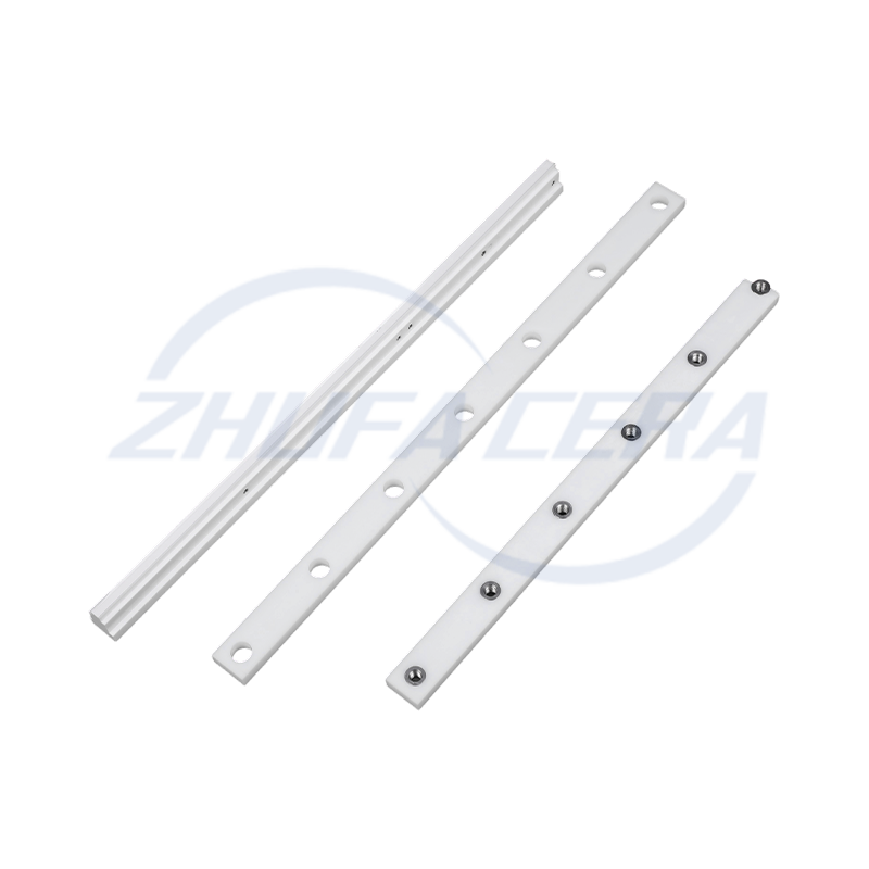
Zirconia Ceramic Guide Rail is a high-performance precision mechanical component made of zirconium oxide ceramic material. Its core characteristics are derived from the excellent physical and chemical...
See Details -
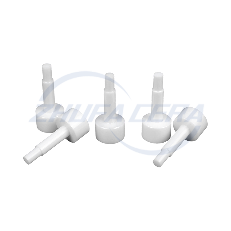
Zirconia Ceramic Locating Pin is a high-precision positioning element made of advanced zirconium oxide ceramic material with excellent physical and chemical properties. Its main characteristics includ...
See Details -
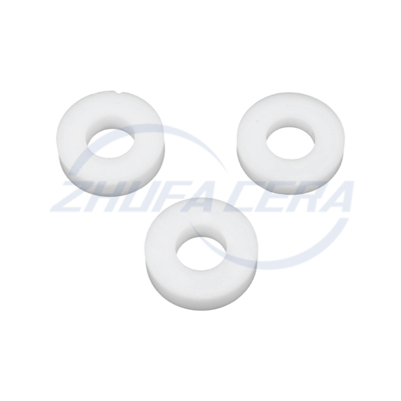
Zirconia Ceramic Ring is a high-performance ceramic product known for its excellent physical and chemical properties. It has extremely high hardness and strength, with a Mohs hardness of more than 8.5...
See Details -
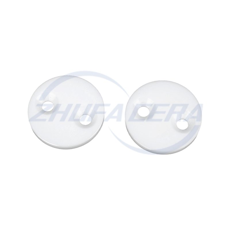
Zirconia ceramic sheets have become functional core components in various fields thanks to their unique properties. With a flexural strength of 900–1200 MPa and a fracture toughness of 6–10 MPa・m¹/², ...
See Details -

Zirconia Ceramic Strip is a strip material made of high-performance zirconium oxide ceramic with excellent physical and chemical properties. It has extremely high hardness and flexural strength, can e...
See Details -
Zirconia ceramic wafers are representative products in the field of high-performance structural ceramics. Compared with traditional alumina ceramics or metal materials, its comprehensive performanc...
See Details -
Zirconia Ceramic Plunger is a high-performance component designed for harsh industrial environments. Compared with similar ceramic or metal plunger products, it stands out with its unique material adv...
See Details

-
Quick Links
Home Products About Us Services Technology News Contact Us -
Products
Ceramic Structural Parts Zirconia Ceramics Alumina Ceramics ZTA Ceramics Silicon Nitride Ceramics Silicon Carbide Ceramics Ceramic Injection Molded Parts -
About Us
Factory Tour Honor FAQ -
Contact info
+86-188 8878 5188zf@zfcera.comNo. 1, Xinggong Road, Anchang Industrial Park, Keqiao District, Shaoxing City, Zhejiang Province, China -
WhatsApp

Copyright © Zhejiang Zhufa Precision Ceramics Technology Co., Ltd. All Rights Reserved.
China precision ceramics manufacturer
wholesale precision ceramics supplier
