
 中文简体
中文简体 русский
 Español
 عربى
عربى Português
 日本語
日本語 한국어
한국어
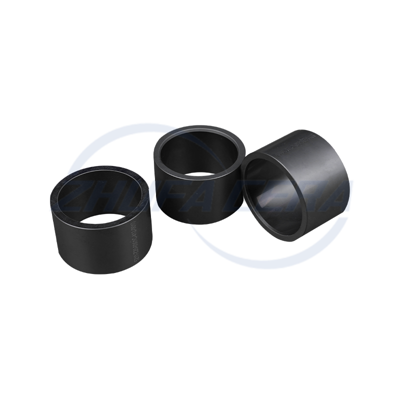
Black silicon carbide ceramic ring is a high-performance engineered ceramic assembly made of high-purity silicon carbide by precision molding and high temperature sintering. Its quadrangular crystal s...
See Details
FOLLOW US :


 Email: zf@zfcera.com
 Telephone: +86-188 8878 5188

Key applications of advanced precision ceramics in semiconductor equipment: in-depth analysis of the properties of high-purity alumina, aluminum nitride and zirconium oxide
2026-03-30
Content
On top of the "crown" of modern industry, semiconductor manufacturing, every nanometer precision leap is inseparable from the underlying support of materials science. As Moore's Law approaches the physical limit, semiconductor equipment has increasingly stringent requirements for high purity, high strength, corrosion resistance, thermal stability and other properties. In this game of the micro world, advanced precision ceramics rely on their Excellent Its physical and chemical properties are moving from behind the scenes to the front, becoming an indispensable key cornerstone to support core processes such as etching (Etch), thin film deposition (PVD/CVD), photolithography (Lithography) and ion implantation.
1. Why do semiconductor equipment prefer precision ceramics?
The semiconductor manufacturing environment has been hailed as one of the “harshest working conditions on earth." In the reaction chamber, materials are subjected to strong acid and alkali chemical corrosion, high-energy plasma bombardment, and severe thermal cycling from room temperature to over 1000°C.
Traditional metal materials (such as aluminum alloys and stainless steel) are prone to physical sputtering in plasma environments, producing metal ion contamination, which directly leads to wafer scrapping; while ordinary polymer materials cannot withstand the outgassing effect in high temperatures and vacuum environments. Precision ceramics are known for their near-zero metal contamination, low linear expansion coefficient and outstanding Chemical inertness has become a key structural component of semiconductor equipment. core Select.
2. Performance game between high-purity alumina, aluminum nitride and zirconia
In the semiconductor field, different working conditions have different emphasis on ceramic materials. At present, high-purity alumina, aluminum nitride and zirconium oxide constitute the three pillars of the application system.
1. High purity alumina
As a widely used structural ceramic, semiconductor grade alumina usually requires a purity of 99.7% or even above 99.9%.
-
Performance advantages: excellent electrical insulation, high mechanical strength and significant Resistant to fluorine-based plasma corrosion.
-
Typical applications: The gas distribution plate (showerhead), ceramic bushing, and wafer handling robot arm in the etching machine.
2. “Thermal Management” important plan ”
Aluminum nitride plays a key role in scenarios that require frequent heating and cooling or high-power heat dissipation.
-
Performance advantages: Its thermal conductivity (usually up to 170-230 W/m·K) is close to that of aluminum metal, and its thermal expansion coefficient (4.5 × 10⁻⁶/°C) is highly close to that of silicon wafers, which can effectively reduce wafer warpage caused by thermal stress.
-
Typical applications: Electrostatic chuck (ESC) substrate, heater (Heater), and substrate packaging.
3. “Strong materials” in ceramics
Zirconia is known for its remarkably high fracture toughness among ceramic materials.
- Performance advantages: Good combination of hardness and toughness, wear resistance highlight , and has low thermal conductivity (suitable for heat insulation scenarios).
- Typical applications: Structural connectors, wear-resistant bearings, thermally insulating supports in vacuum environments.
3. Strive for excellence to empower core components
1. Electrostatic chuck (ESC), the “core carrier” of advanced manufacturing processes
In etching and ion implantation equipment, electrostatic chucks attract wafers through Coulomb forces. At its core is a multilayer structure made of high-purity aluminum oxide or aluminum nitride. Precision ceramics not only provide insulation protection, but also achieve precise control of wafer temperature (accuracy up to ±0.1°C) through internally embedded electrodes and cooling channels.
2. Etch the components inside the cavity to form a “barrier” against plasma
During the etching process, high-energy plasma will continuously bombard the cavity. Precision components using high-purity alumina or yttrium-based ceramic coatings can significantly reduce the particle generation rate. Experimental data shows that using high-purity ceramics instead of traditional materials can extend the equipment maintenance cycle (MTBC) by more than 30%.
3. Precision shift stage of photolithography machine, pursuing precise positioning
The photolithography machine's positioning accuracy requirement for the workpiece stage is at the sub-nanometer level. Ceramic materials with high specific stiffness, low thermal expansion, and high damping characteristics ensure that the stage is not easily deformed due to inertia or heat during high-speed movement, ensuring the alignment accuracy of exposure.
4. Independent innovation helps the future of the industry
He who observes the situation is wise, and he who controls the situation wins. Currently, the semiconductor industry is in a critical window period for technological iteration. Large size, integration, and localization have become inevitable trends in the development of the precision ceramics industry.
-
Large size: Large-sized ceramic components adapted to wafers of 12 inches and above pose higher challenges to the molding and sintering processes.
-
Integration: The integrated integration of structural parts and sensor heating functions is pushing ceramic components from single "mechanical parts" to "intelligent modules".
-
Localization: Today, when supply chain security is of great concern, realizing independent control of the entire industrial chain from high-purity powder to precision processing has become the mission of the times for key enterprises in the industry such as Zhufa Technology.
Conclusion
Precision ceramics may seem cold and simple, but they actually contain the power to change the microscopic world. From the iteration of basic materials to the life optimization of core components, every technological breakthrough is a tribute to high-precision manufacturing.
As someone deeply involved in the field of advanced ceramics important strength, Zhufa Precision Ceramic Technology Co., Ltd. We always adhere to technological innovation as our core and are committed to providing high reliability, long-life precision ceramic solutions to semiconductor partners. We know that only by continuously pursuing quality can we live up to the important responsibilities entrusted by the times.
[Technical consultation and selection support]
If you are looking for information about High-performance ceramic chuck customization, plasma-resistant component solutions or advanced process material replacement For professional solutions, please contact Zhufa Technology. We will provide you with detailed material ICP-MS test reports, complex structural parts process evaluation and selection suggestions. 
Related products
-
-
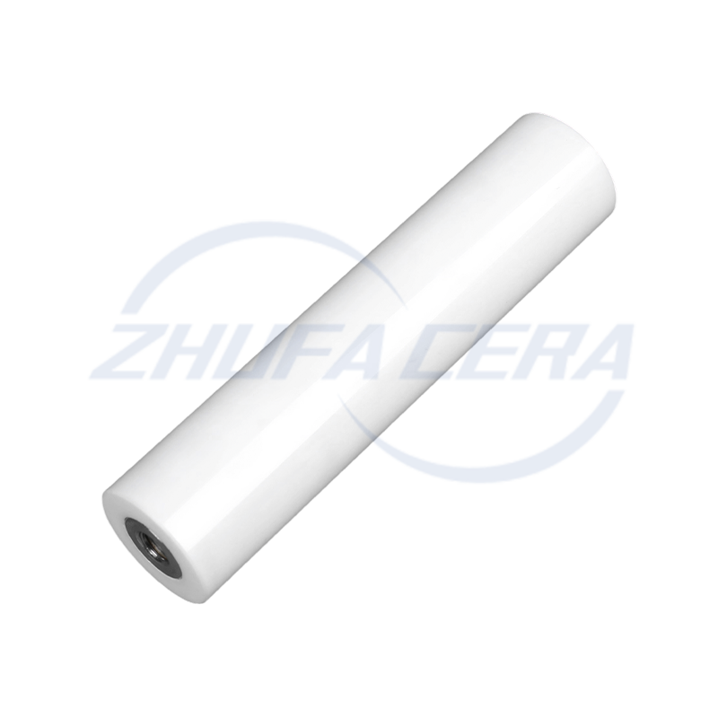
Zirconia Ceramic Rod is a high-performance ceramic material rod, mainly made of zirconium oxide, with excellent mechanical strength and chemical stability. It exhibits extremely high hardness and wear...
See Details -
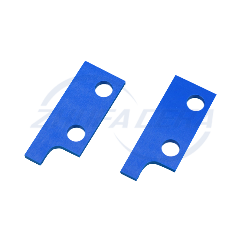
Blue zirconia ceramic sheets are precision components made of advanced zirconia ceramics. They are stained with cobalt, iron or copper to form a blue color. This color not only serves as a visual i...
See Details -

This blue zirconia ceramic pin is made of advanced zirconia ceramic material, providing excellent durability and performance. Zirconia ceramics are known for their high strength, good wear resistan...
See Details -

Zirconia Ceramic Gear is made of zirconium oxide ceramic material, which has excellent high strength and high hardness. This material property enables it to effectively resist wear during the transmis...
See Details -
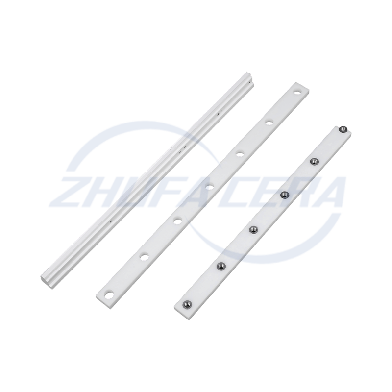
Zirconia Ceramic Guide Rail is a high-performance precision mechanical component made of zirconium oxide ceramic material. Its core characteristics are derived from the excellent physical and chemical...
See Details -
Zirconia Ceramic Locating Pin is a high-precision positioning element made of advanced zirconium oxide ceramic material with excellent physical and chemical properties. Its main characteristics includ...
See Details -
Zirconia Ceramic Ring is a high-performance ceramic product known for its excellent physical and chemical properties. It has extremely high hardness and strength, with a Mohs hardness of more than 8.5...
See Details -
Zirconia ceramic sheets have become functional core components in various fields thanks to their unique properties. With a flexural strength of 900–1200 MPa and a fracture toughness of 6–10 MPa・m¹/², ...
See Details -

Zirconia Ceramic Strip is a strip material made of high-performance zirconium oxide ceramic with excellent physical and chemical properties. It has extremely high hardness and flexural strength, can e...
See Details -
Zirconia ceramic wafers are representative products in the field of high-performance structural ceramics. Compared with traditional alumina ceramics or metal materials, its comprehensive performanc...
See Details -
Zirconia Ceramic Plunger is a high-performance component designed for harsh industrial environments. Compared with similar ceramic or metal plunger products, it stands out with its unique material adv...
See Details

-
Quick Links
Home Products About Us Services Technology News Contact Us -
Products
Ceramic Structural Parts Zirconia Ceramics Alumina Ceramics ZTA Ceramics Silicon Nitride Ceramics Silicon Carbide Ceramics Ceramic Injection Molded Parts -
About Us
Factory Tour Honor FAQ -
Contact info
+86-188 8878 5188zf@zfcera.comNo. 1, Xinggong Road, Anchang Industrial Park, Keqiao District, Shaoxing City, Zhejiang Province, China -
WhatsApp

Copyright © Zhejiang Zhufa Precision Ceramics Technology Co., Ltd. All Rights Reserved.
China precision ceramics manufacturer
wholesale precision ceramics supplier
