中文简体
中文简体 русский
 Español
 عربى
عربى Português
 日本語
日本語 한국어
한국어


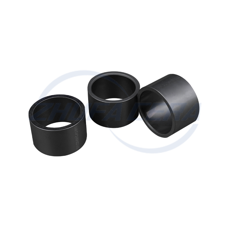
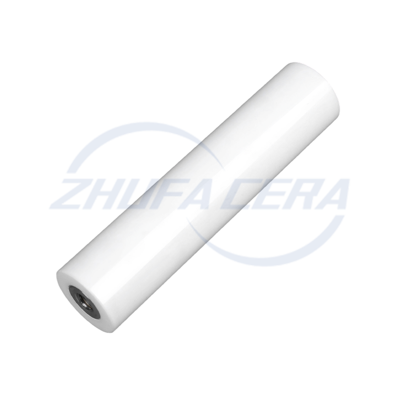
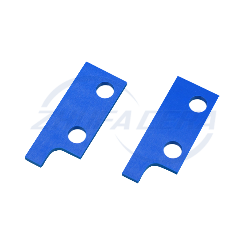
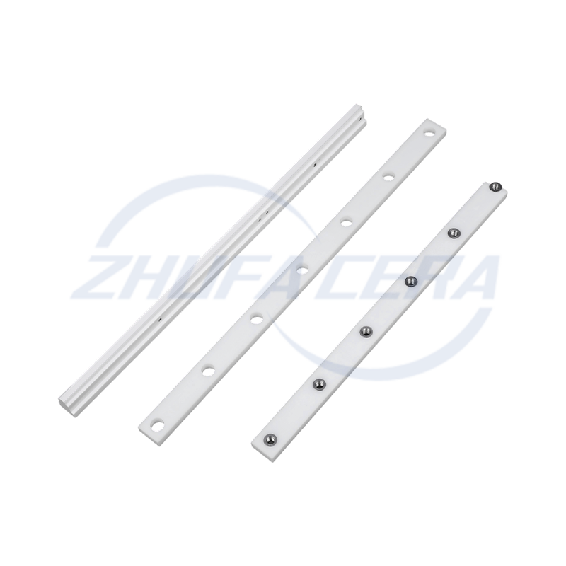
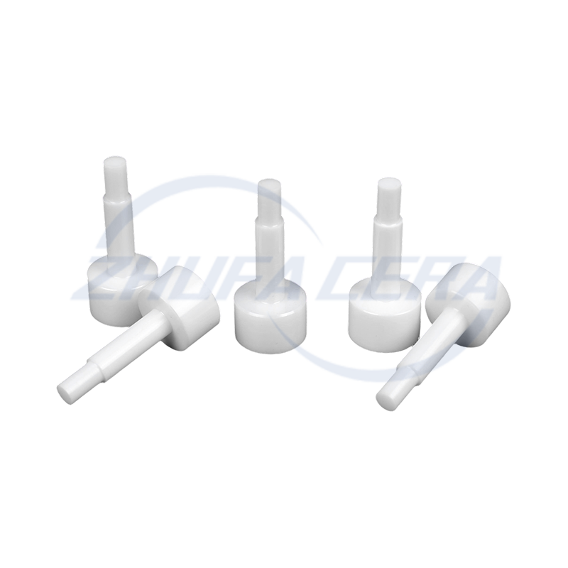
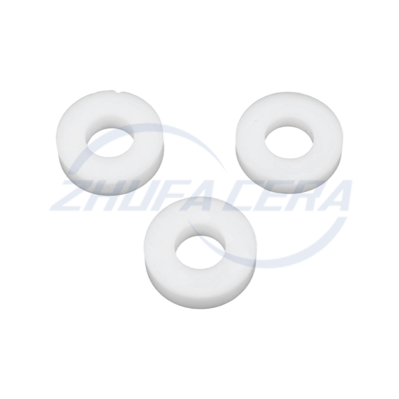
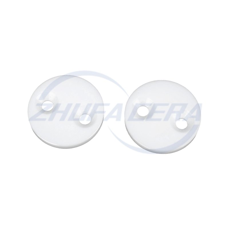
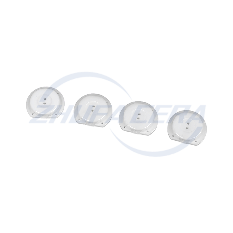
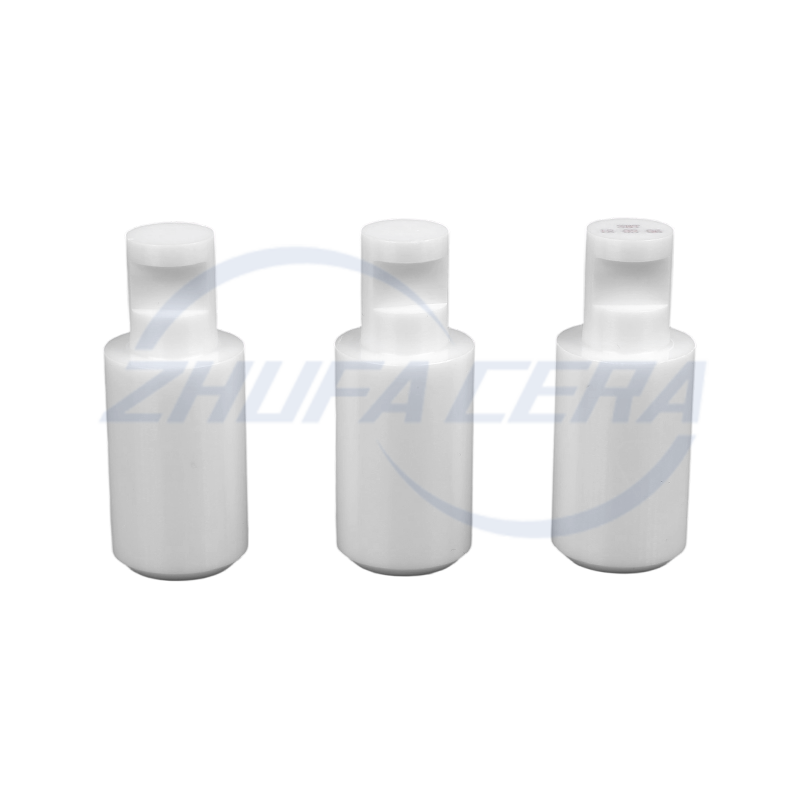
Custom Shape Alumina Ceramic Rod is a customized ceramic component with high-purity alumina (Al₂O₃ content ≥ 99.9%) as the main body. Its core advantage lies in the one-time molding of non-standard shapes through precision molding technology. Compared with traditional standard cylindrical ceramic rods, the special-shaped design can directly adapt to complex mechanical structures, reduce subsequent processing steps such as cutting and grinding, and significantly reduce assembly errors and costs. For example, in semiconductor etching equipment, its optimized flow channel design can improve the uniformity of gas distribution and increase the wafer yield by 4.7%; in the aerospace field, its lightweight characteristics (density is only half of that of steel) help satellite attitude adjustment mechanisms reduce weight by 30% while maintaining a positioning accuracy of ±1μm. This "design is the finished product" feature makes it an irreplaceable choice in extreme industrial scenarios that require high precision, high corrosion resistance, and high temperature resistance.
1. Material properties: the cornerstone of performance
High purity and corrosion resistance: Using 99.9% alumina raw material, it has excellent resistance to corrosive media such as acid, alkali, and salt, and is suitable for strong chemical environments such as lithium battery electrolyte transportation and chemical reactors.
Thermal stability: The melting point is as high as 2050℃, the thermal conductivity is 20-30W/m·K, and it can work continuously at 1700℃. It is an ideal material for the inner lining of the combustion chamber of an aircraft engine and thermal protection tiles.
Electrical insulation: The volume resistivity is 10¹⁴Ω·cm, and the breakdown voltage is 10kV/mm, which ensures the safety of semiconductor equipment under high-voltage environment. It is widely used in electrostatic chucks and etching cavity linings.
2. Manufacturing process: guarantee of precision
Precision molding: Through dry pressing, grouting or 3D printing process, complex shapes can be formed in one time, and the gradient sintering technology is combined to control the 200mm length error ≤2μm, meeting the nano-level precision requirements of the core components of the lithography machine.
Surface treatment: Diamond micro-powder grinding (surface roughness Ra≤0.1μm) or laser processing is used to adapt to the strict requirements of semiconductor equipment for low friction and high flatness.
3. Application scenarios: cross-field solutions
Semiconductor field: As a manipulator transmission shaft, it can achieve 300 times of ±1μm repeated positioning per hour; as a ceramic heater, it can ensure the temperature uniformity of the wafer deposition process.
Medical field: used for artificial joints (ZTA composite materials enhance toughness) and dental implants, with excellent biocompatibility, significantly reducing the risk of osteolysis and rejection.
New energy field: BYD blade battery uses directional heat-conducting ceramic components to control the temperature difference of the battery pack within ±2℃, solving the risk of thermal runaway.
4. Technological breakthrough: innovation drives value
Lightweight design: While reducing the weight of satellite transmission components by 30%, it maintains an accuracy of ±1μm and improves the payload efficiency of spacecraft.
Long-life maintenance: Chemical pipeline lining reduces maintenance costs by 70%, extends the equipment maintenance cycle to 18 months, and reduces the cost of the entire life cycle.